

herunterladen
© Semiconductor Components Industries, LLC, 2013
November, 2013 − Rev. 1
1 Publication Order Number:
NCP45560/D
NCP45560
ecoSWITCHt
Advanced Load Management
Controlled Load Switch with Low R
ON
The NCP45560 load switch provides a component and
area-reducing solution for efficient power domain switching with
inrush current limit via soft−start. In addition to integrated control
functionality with ultra low on−resistance, this device offers system
safeguards and monitoring via fault protection and power good
signaling. This cost effective solution is ideal for power management
and hot-swap applications requiring low power consumption in a
small footprint.
Features
• Advanced Controller with Charge Pump
• Integrated N-Channel MOSFET with Ultra Low R
ON
• Input Voltage Range 0.5 V to 13.5 V
• Soft-Start via Controlled Slew Rate
• Adjustable Slew Rate Control
• Power Good Signal
• Thermal Shutdown
• Undervoltage Lockout
• Short-Circuit Protection
• Extremely Low Standby Current
• Load Bleed (Quick Discharge)
• This is a Pb−Free Device
Typical Applications
• Portable Electronics and Systems
• Notebook and Tablet Computers
• Telecom, Networking, Medical, and Industrial Equipment
• Set−Top Boxes, Servers, and Gateways
• Hot−Swap Devices and Peripheral Ports
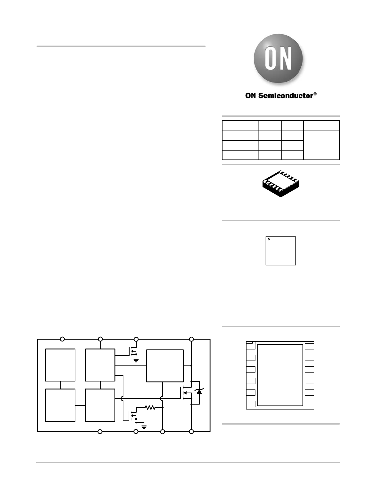
Figure 1. Block Diagram
EN
Bandgap
&
Biases
Charge
Pump
Delay and
Slew Rate
Control
GND
BLEED
Thermal,
Undervoltage
&
Short−Circuit
Protection
SR
Control
Logic
PG
V
OUT
V
IN
V
CC
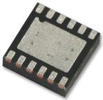
DFN12, 3x3
CASE 506CD
MARKING DIAGRAM
http://onsemi.com
R
ON
TYP V
CC
I
MAX
2.4 mW
3.3 V
24 A
3.3 V
2.6 mW
V
IN
1.8 V
5.0 V
PIN CONFIGURATION
(Top View)
See detailed ordering and shipping information on page 12 of
this data sheet.
ORDERING INFORMATION
(Note: Microdot may be in either location)
3.2 mW
3.3 V 12 V
1
EN
GND
4
2
3
12
11
10
9
13: V
IN
V
OUT
V
OUT
V
CC
V
IN
NCP45
560−x
ALYWG
G
SR
5
8
PG
BLEED
6
7
V
OUT
V
OUT
1
V
OUT
x = H for NCP45560−H
= L for NCP45560−L
A = Assembly Location
L = Wafer Lot
Y = Year
W = Work Week
G = Pb−Free Package
Verzeichnis
- ・ Konfiguration des Pinbelegungsdiagramms on Seite 1 Seite 2
- ・ Abmessungen des Paketumrisses on Seite 13
- ・ Paket-Footprint-Pad-Layout on Seite 13
- ・ Teilenummerierungssystem on Seite 1 Seite 12 Seite 13
- ・ Markierungsinformationen on Seite 1 Seite 13
- ・ Blockdiagramm on Seite 1
- ・ Typisches Anwendungsschaltbild on Seite 1 Seite 11 Seite 12
- ・ Technische Daten on Seite 2 Seite 12
- ・ Anwendungsbereich on Seite 1 Seite 3 Seite 10
- ・ Elektrische Spezifikation on Seite 3