
herunterladen
© Semiconductor Components Industries, LLC, 2008
February, 2008 - Rev. 1
1 Publication Order Number:
AND8172/D
AND8172/D
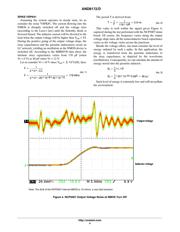
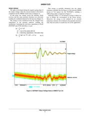
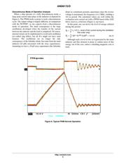
Understanding the Noise
Issue Out of Inductor Based
DC-DC Converter
Prepared by: Michael Bairanzade
ON Semiconductor
Abstract
Portable applications, such as cellular phones and
hand-held computers, have sensitive electronic functions,
making any electromagnetic noise a real issue. Even a low
power converter can generate noise during transients since
the converters operate in the megahertz range. The high
frequency switching can interact with the parasitic circuit
elements to create uncontrolled noise. In addition, the
associated voltage spikes might be difficult to filter out, a
detailed analysis of the converter operation being necessary
to properly design the system. Of course, the mechanical
layout is a key parameter to minimize the EMI perturbation.
The main purpose of this document is to clarify the source of
such a noise, and assess the risk of system's EMI pollution.
The NCP5007 device, together with a PWM based structure,
will be used as vehicles to perform the associated
engineering test in a real application, but the same may apply
to other Boost converters, such as the NCP5005.
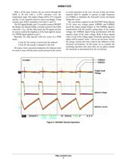
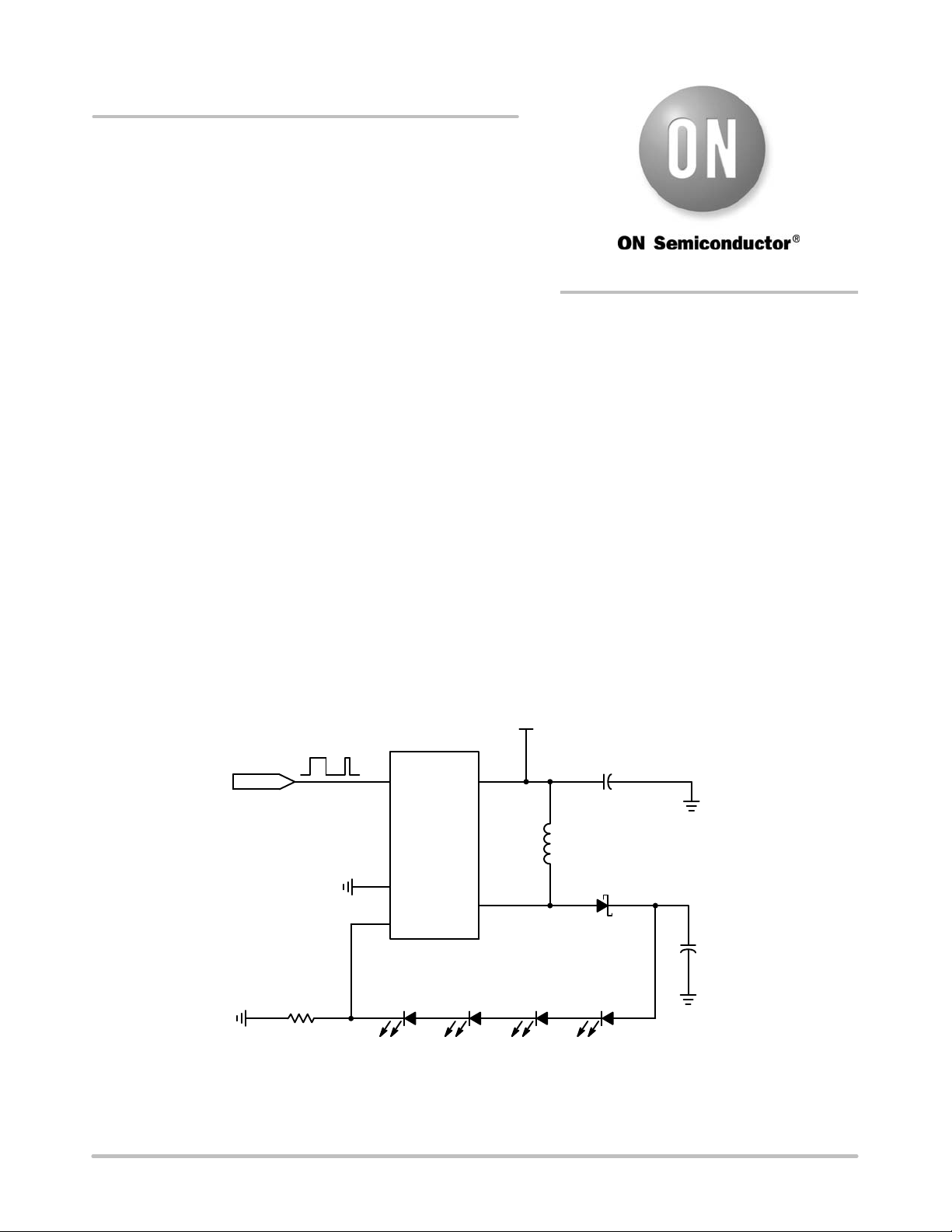
NCP5007/NCP5005 Basic Analysis
The NCP5007/NCP5005 are dc-dc converters dedicated
to the supply of High Efficiency White LEDs used as an
LCD back light or photo flash light source. Generally
speaking, with a typical 3.8 V Vf drop during normal
operation, these LEDs are not capable to operate from a
standard 3.6 V battery pack. A boost circuit must be
provided to raise the voltage up to the bias called by such a
diode. Moreover, these LEDs are commonly connected in
series to get a constant current through the diodes, assuring
smooth and consistent light across the LCD panel.
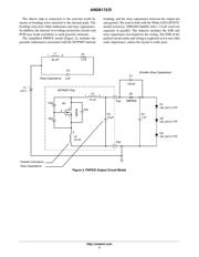
The basic application, depicted in Figure 1, drives the
back light of a standard LCD display, the command bit EN
being provided by an external CPU or other digital
controller.
EN
GND
3
U1
V
bat
5
2
GND
FB
1
V
out
4
NCP5007
47 W
R1
GND
LWT67C
D5
LWT67C
D4
LWT67C
D3
LWT67C
D2
MBR0530
D1
22 mH
L1
V
bat
C1
4.7 mF
GND
GND
C2
1.0 mF
Figure 1. Typical Back Light Application
Pulse
APPLICATION NOTE
http://onsemi.com
Verzeichnis