


herunterladen
© Semiconductor Components Industries, LLC, 2009
September, 2009 − Rev. 14
1 Publication Order Number:
NCP565/D
NCP565/NCV565
1.5 A Low Dropout
Linear Regulator
The NCP565/NCV565 low dropout linear regulator will provide
1.5 A at a fixed output voltage or an adjustable voltage down to 0.9 V.
The fast loop response and low dropout voltage make this regulator
ideal for applications where low voltage and good load transient
response are important. Device protection includes current limit, short
circuit protection, and thermal shutdown.
Features
• Ultra Fast Transient Response (t1.0 ms)
• Low Ground Current (1.5 mA at Iload = 1.5 A)
• Low Dropout Voltage (0.9 V at Iload = 1.5 A)
• Low Noise (28 mVrms)
• 0.9 V Reference Voltage
• Adjustable Output Voltage from 7.7 V down to 0.9 V
• 1.2 V, 1.5 V, 2.8 V, 3.0 V, 3.3 V Fixed Output Versions. Other Fixed
Voltages Available on Request
• Current Limit Protection (3.3 A Typ)
• Thermal Shutdown Protection (160°C)
• NCV Prefix for Automotive and Other Applications Requiring Site
and Change Controls
• Pb−Free Packages are Available
Typical Applications
• Servers
• ASIC Power Supplies
• Post Regulation for Power Supplies
• Constant Current Source
http://onsemi.com
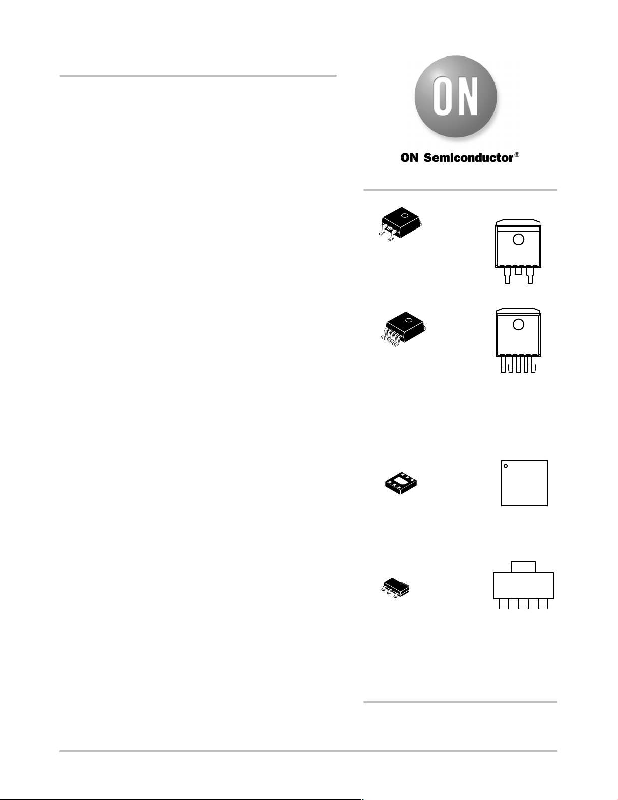
D
2
PAK 5
CASE 936A
ADJUSTABLE
1
5
Tab = Ground
Pin 1. N.C.
2. V
in
3. Ground
4. V
out
5. Adj
xx = 12 or 33
y = P or V
A = Assembly Location
WL = Wafer Lot
Y = Year
WW = Work Week
G = Pb−Free
See detailed ordering and shipping information in the package
dimensions section on page 13 of this data sheet.
ORDERING INFORMATION
1
2
3
D
2
PAK 3
CASE 936
FIXED
MARKING
DIAGRAMS
Tab = Ground
Pin 1. V
in
2. Ground
3. V
out
NC
P565D2Txx
AWLYWWG
NC
y565D2T
AWLYWWG
DFN6, 3x3.3
CASE 506AX
yy = Voltage Rating
12 = 1.2 V
A = Assembly Location
Y = Year
W = Work Week
G = Pb−Free Package
P565
MNxx
AYWWG
G
1
1
AYW
565yy G
G
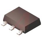
SOT−223
CASE 318E
(Note: Microdot may be in either location)
xx = Voltage Rating
AJ = Adjustable
12 = 1.2 V
15 = 1.5 V
28 = 2.8 V
Tab = V
out
Pin 1. Ground
2. V
out
3. V
in
30 = 3.0V
33 = 3.3 V
Verzeichnis
- ・ Konfiguration des Pinbelegungsdiagramms on Seite 2
- ・ Abmessungen des Paketumrisses on Seite 14 Seite 15 Seite 16 Seite 17
- ・ Paket-Footprint-Pad-Layout on Seite 14 Seite 15 Seite 16 Seite 17
- ・ Teilenummerierungssystem on Seite 1 Seite 13 Seite 17
- ・ Markierungsinformationen on Seite 1
- ・ Blockdiagramm on Seite 2 Seite 8 Seite 9
- ・ Typisches Anwendungsschaltbild on Seite 1 Seite 2 Seite 9
- ・ Technische Daten on Seite 3 Seite 13
- ・ Anwendungsbereich on Seite 1
- ・ Elektrische Spezifikation on Seite 3 Seite 4