


herunterladen

© Semiconductor Components Industries, LLC, 2016
August, 2016 − Rev. 5
1 Publication Order Number:
NCV7428/D
NCV7428
System Basis Chip with
Integrated LIN and Voltage
Regulator
Description
NCV7428 is a System Basis Chip (SBC) integrating functions
typically found in automotive Electronic Control Units (ECUs).
NCV7428 provides and monitors the low−voltage power supply for
the application microcontroller and other loads and includes a LIN
transceiver.
Features
• Control Logic
♦ Ensures safe power−up sequence and the correct reaction to
different supply conditions
♦ Controls mode transitions including the power management and
bus wakeup treatment
♦ Generates reset
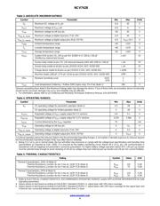
• 3.3 V or 5 V V
OUT
Supply depending on the Version from a
Low−drop Voltage Regulator
♦ Can deliver up to 70 mA with accuracy of ±2%
♦ Supplies typically the ECU’s microcontroller
♦ Undervoltage detector with a reset output to the supplied
microcontroller
• LIN Transceiver
♦ LIN2.x and J2602 compliant
♦ TxD dominant timeout protection
♦ Transceiver mode controlled by dedicated input pin
• Protection and Monitoring Functions
♦ Thermal shutdown protection
♦ Load dump protection (45 V)
♦ LIN Bus pin protected against transients in an automotive
environment
♦ ESD protection level for LIN and V
S
> ±8 kV
• Wettable Flank Package for Enhanced Optical Inspection
Quality
• NCV Prefix for Automotive and Other Applications Requiring
Unique Site and Control Change Requirements; AEC−Q100
Qualified and PPAP Capable
• These Devices are Pb−Free, Halogen Free/BFR Free and are RoHS
Compliant
Typical Applications
• Automotive
• Industrial Networks
www.onsemi.com
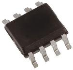
(Top View)
5
6
7
8
1
2
3
4
GND
LIN
EN
TxD
See detailed ordering, marking and shipping information in the
package dimensions section on page 17 of this data sheet.
ORDERING INFORMATION
V
S
RxD
RSTN
PIN ASSIGNMENT
MARKING DIAGRAMS
1
8
SOIC−8
D SUFFIX
CASE 751AZ
A = Assembly Location
L = Wafer Lot
Y = Year
W = Work Week
G = Pb−Free Package
NV7428xx
ALYW G
G
1
8
NCV7428
(Note: Microdot may be in either location)
V
OUT
DFN8
MW SUFFIX
CASE 506DG
1
NV7428xx
ALYWG
G
1
Verzeichnis
- ・ Konfiguration des Pinbelegungsdiagramms on Seite 1 Seite 2
- ・ Abmessungen des Paketumrisses on Seite 18 Seite 19
- ・ Paket-Footprint-Pad-Layout on Seite 18 Seite 19
- ・ Teilenummerierungssystem on Seite 1 Seite 17 Seite 19
- ・ Markierungsinformationen on Seite 1 Seite 17 Seite 19
- ・ Blockdiagramm on Seite 2
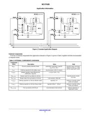
- ・ Typisches Anwendungsschaltbild on Seite 1
- ・ Beschreibung der Funktionen on Seite 9
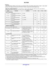
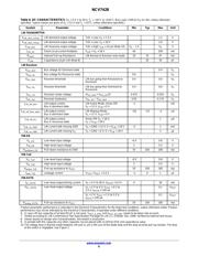
- ・ Technische Daten on Seite 4 Seite 17
- ・ Anwendungsbereich on Seite 1
- ・ Elektrische Spezifikation on Seite 4 Seite 5 Seite 6 Seite 7
- ・ Teilenummernliste on Seite 4