


May 2002
2002 Fairchild Semiconductor Corporation
NDC7001C Rev B (W)
NDC7001C
Dual N & P-Channel Enhancement Mode Field Effect Transistor
General Description
These dual N & P-Channel Enhancement Mode Field
Effect Transistors are produced using Fairchild’s
proprietary, high cell density, DMOS technology. This
very high density process has been designed to
minimize on-state resistance, provide rugged and
reliable performance and fast switching. These
device is particularly suited for low voltage, low
current, switching, and power supply applications.
Features
• Q1 0.51 A, 60V. R
DS(ON)
= 2 Ω @ V
GS
= 10 V
R
DS(ON)
= 4 Ω @ V
GS
= 4.5 V
• Q2 –0.34 A, 60V. R
DS(ON)
= 5 Ω @ V
GS
= –10 V
R
DS(ON)
= 7.5Ω @ V
GS
= –4.5 V
• High saturation current
• High density cell design for low R
DS(ON)
• Proprietary SuperSOT
TM
–6 package: design using copper
lead frame for superior thermal and electrical capabilities
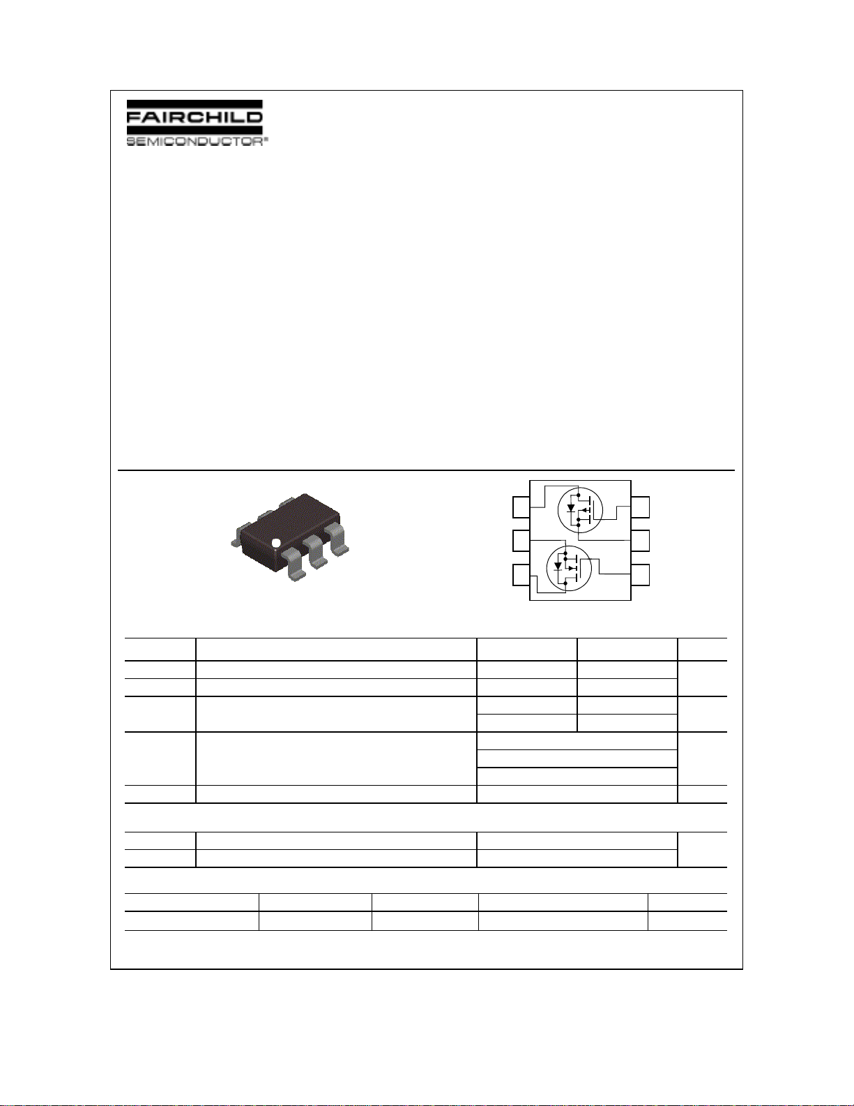
D1
S2
G1
D2
S1
G2
SuperSOT -6
TM
3
2
1
4
5
6
Q1(N)
Q2(P)
Absolute Maximum Ratings T
A
=25
o
C unless otherwise noted
Symbol Parameter Q1 Q2 Units
V
DSS
Drain-Source Voltage 60 –60 V
V
GSS
Gate-Source Voltage
±20 ±20
I
D
Drain Current – Continuous (Note 1a) 0.51 –0.34 A
– Pulsed 1.5 –1
Power Dissipation for Single Operation (Note 1a) 0.96
(Note 1b)
0.9
P
D
(Note 1c)
0.7
W
T
J
, T
STG
Operating and Storage Junction Temperature Range –55 to +150
°C
Thermal Characteristics
R
θJA
Thermal Resistance, Junction-to-Ambient
(Note 1a) 130
°C/W
R
θJC
Thermal Resistance, Junction-to-Case
(Note 1) 60
Package Marking and Ordering Information
Device Marking Device Reel Size Tape width Quantity
.01C NDC7001C 7’’ 8mm 3000
NDC7001C
Verzeichnis