


herunterladen
© Semiconductor Components Industries, LLC, 2009
May, 2009 − Rev. 3
1 Publication Order Number:
NSR0140P2/D
NSR0140P2T5G
Schottky Barrier Diode
These Schottky barrier diodes are designed for high−speed
switching applications, circuit protection, and voltage clamping.
Extremely low forward voltage reduces conduction loss. Miniature
surface mount package is excellent for hand−held and portable
applications where space is limited.
Features
• Extremely Fast Switching Speed
• Extremely Low Forward Voltage − 0.28 V (Typ) @ I
F
= 1.0 mA
• Low Reverse Current
• Lead−Free Plating
• This is a Pb−Free Device
MAXIMUM RATINGS
Rating Symbol Value Unit
Repetitive Peak Reverse Voltage V
RM
40 V
Continuous Reverse Voltage (DC) V
R
30 V
Continuous Forward Current (DC) I
F
70 mA
Non−Repetitive Peak Forward Surge Current I
FSM
500 mA
ESD Rating: Class 1C per Human Body Model
Class A per Machine Model
Stresses exceeding Maximum Ratings may damage the device. Maximum
Ratings are stress ratings only. Functional operation above the Recommended
Operating Conditions is not implied. Extended exposure to stresses above the
Recommended Operating Conditions may affect device reliability.
THERMAL CHARACTERISTICS
Characteristic Symbol Max Unit
Total Device Dissipation FR−5 Board,
(Note 1) T
A
= 25°C
Derate above 25°C
P
D
100
1.0
mW
mW/°C
Thermal Resistance,
Junction−to−Ambient
R
q
JA
1000 °C/W
Junction and Storage
Temperature Range
T
J
, T
stg
−55 to +125 °C
1. FR−5 Minimum Pad.
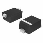
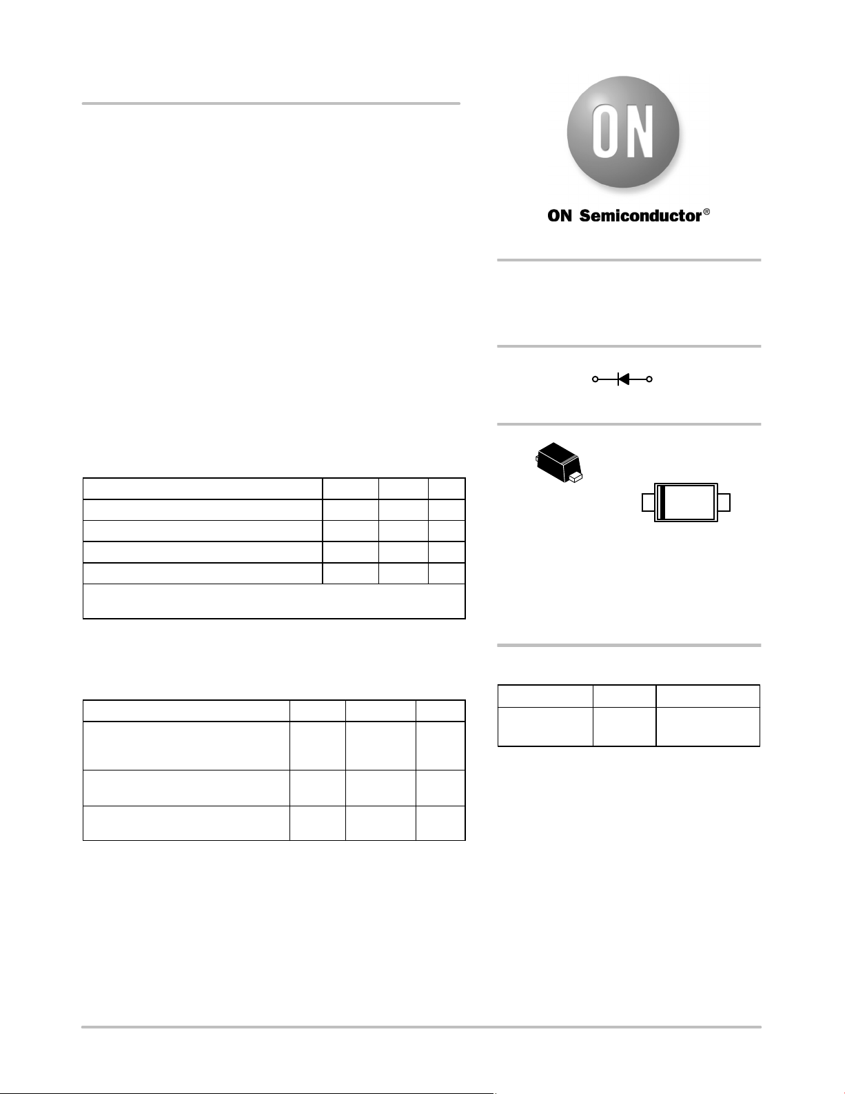
40 V SCHOTTKY
BARRIER DIODE
1
CATHODE
2
ANODE
http://onsemi.com
Device Package Shipping†
ORDERING INFORMATION
NSR0140P2T5G SOD−923
(Pb−Free)
8000/Tape & Reel
†For information on tape and reel specifications,
including part orientation and tape sizes, please
refer to our Tape and Reel Packaging Specifications
Brochure, BRD8011/D.
SOD−923
CASE 514AA
PLASTIC
M = Specific Device Code*
(Character is rotated 270° clockwise)
M = Month Code
G = Pb−Free Package
(Note: Microdot may be in either location)
MARKING
DIAGRAM
M MG
G
1
2
12
Verzeichnis