
herunterladen

© Semiconductor Components Industries, LLC, 2005
October, 2016 − Rev. 4
1 Publication Order Number:
NSS30100L/D
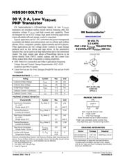
NSS30100LT1G
30 V, 2 A, Low V
CE(sat)
PNP Transistor
ON Semiconductor’s e
2
PowerEdge family of low V
CE(sat)
transistors are miniature surface mount devices featuring ultra low
saturation voltage (V
CE(sat)
) and high current gain capability. These
are designed for use in low voltage, high speed switching applications
where affordable efficient energy control is important.
Typical application are DC−DC converters and power management
in portable and battery powered products such as cellular and cordless
phones, PDAs, computers, printers, digital cameras and MP3 players.
Other applications are low voltage motor controls in mass storage
products such as disc drives and tape drives. In the automotive
industry they can be used in air bag deployment and in the instrument
cluster. The high current gain allows e
2
PowerEdge devices to be
driven directly from PMU’s control outputs, and the Linear Gain
(Beta) makes them ideal components in analog amplifiers.
• NSV Prefix for Automotive and Other Applications Requiring
Unique Site and Control Change Requirements; AEC−Q101
Qualified and PPAP Capable
• These Devices are Pb−Free, Halogen Free/BFR Free and are RoHS
Compliant
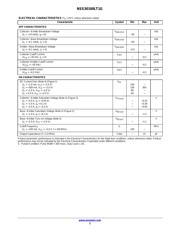
MAXIMUM RATINGS (T
A
= 25°C)
Rating
Symbol Max Unit
Collector-Emitter Voltage V
CEO
−30 Vdc
Collector-Base Voltage V
CBO
−50 Vdc
Emitter-Base Voltage V
EBO
−5.0 Vdc
Collector Current − Continuous I
C
−1.0 A
Collector Current − Peak I
CM
−2.0 A
THERMAL CHARACTERISTICS
Characteristic Symbol Max Unit
Total Device Dissipation
T
A
= 25°C
Derate above 25°C
P
D
(Note 1) 310
2.5
mW
mW/°C
Thermal Resistance,
Junction to Ambient
R
θ
JA
(Note 1) 403 °C/W
Total Device Dissipation
T
A
= 25°C
Derate above 25°C
P
D
(Note 2) 710
5.7
mW
mW/°C
Thermal Resistance,
Junction to Ambient
R
θ
JA
(Note 2) 176 °C/W
Total Device Dissipation
(Single Pulse < 10 sec.)
P
Dsingle
(Note 3)
575 mW
Junction and Storage
Temperature Range
T
J
, T
stg
−55 to
+150
°C
Stresses exceeding those listed in the Maximum Ratings table may damage the
device. If any of these limits are exceeded, device functionality should not be
assumed, damage may occur and reliability may be affected.
1. FR−4 @ Minimum Pad.
2. FR−4 @ 1.0 X 1.0 inch Pad.
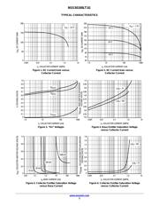
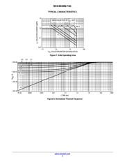
3. Refer to Figure 8.
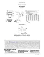
Device Package Shipping
†
ORDERING INFORMATION
NSS30100LT1G,
NSV30100LT1G
SOT−23
(Pb−Free)
3000/Tape & Ree
l
COLLECTOR
3
1
BASE
2
EMITTER
SOT−23 (TO−236)
CASE 318
STYLE 6
3
2
1
30 VOLTS
2.0 AMPS
PNP LOW V
CE(sat)
TRANSISTOR
EQUIVALENT R
DS(on)
200 mW
†For information on tape and reel specifications,
including part orientation and tape sizes, please
refer to our Tape and Reel Packaging Specification
Brochure, BRD8011/D.
MARKING DIAGRAM
1
VS4M G
G
VS4 = Specific Device Code
M = Date Code*
G = Pb−Free Package
*Date Code orientation and/or overbar may
vary depending upon manufacturing location.
(Note: Microdot may be in either location)
www.onsemi.com
Verzeichnis
- ・ Abmessungen des Paketumrisses on Seite 5
- ・ Paket-Footprint-Pad-Layout on Seite 5
- ・ Teilenummerierungssystem on Seite 1 Seite 5
- ・ Markierungsinformationen on Seite 1 Seite 5
- ・ Typisches Anwendungsschaltbild on Seite 1
- ・ Anwendungsbereich on Seite 1
- ・ Elektrische Spezifikation on Seite 2
- ・ Teilenummernliste on Seite 1