


© Semiconductor Components Industries, LLC, 2006
May, 2006 − Rev. 4
1 Publication Order Number:
NTA4151P/D
NTA4151P, NTE4151P
Small Signal MOSFET
−20 V, −760 mA, Single P−Channel,
Gate Zener, SC−75, SC−89
Features
• Low R
DS(on)
for Higher Efficiency and Longer Battery Life
• Small Outline Package (1.6 x 1.6 mm)
• SC−75 Standard Gullwing Package
• ESD Protected Gate
• Pb−Free Packages are Available
Applications
• High Side Load Switch
• DC−DC Conversion
• Small Drive Circuits
• Battery Operated Systems such as Cell Phones, PDAs, Digital
Cameras, etc.
MAXIMUM RATINGS (T
J
= 25°C unless otherwise stated)
Parameter Symbol Value Units
Drain−to−Source Voltage V
DSS
−20 V
Gate−to−Source Voltage V
GS
±6.0 V
Continuous Drain Current
(Note 1)
Steady State I
D
−760 mA
Power Dissipation (Note 1)
SC−75
SC−89
Steady State
P
D
301
313
mW
Pulsed Drain Current
tp =10 ms
I
DM
±1000 mA
Operating Junction and Storage Temperature T
J
,
T
STG
−55 to
150
°C
Continuous Source Current (Body Diode) I
S
−250 mA
Lead Temperature for Soldering Purposes
(1/8 in from case for 10 s)
T
L
260 °C
Gate−to−Source ESD Rating −
(Human Body Model, Method 3015)
ESD 1800 V
THERMAL RESISTANCE RATINGS
Junction−to−Ambient − Steady State (Note 1)
SC−75
SC−89
R
q
JA
415
400
°C/W
Stresses exceeding Maximum Ratings may damage the device. Maximum
Ratings are stress ratings only. Functional operation above the Recommended
Operating Conditions is not implied. Extended exposure to stresses above the
Recommended Operating Conditions may affect device reliability.
1. Surface mounted on FR4 board using 1 in sq pad size (Cu area = 1.127 in sq
[1 oz] including traces).
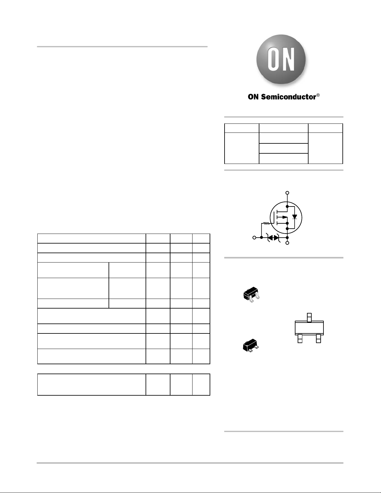
MARKING DIAGRAM
& PIN ASSIGNMENT
http://onsemi.com
xx = Device Code
M = Date Code*
G = Pb−Free Package
(Note: Microdot may be in either location)
*Date Code orientation may vary depending
upon manufacturing location.
xx M G
G
R
DS(on)
TYP I
D
MAXV
(BR)DSS
0.26 W @ −4.5 V
−20 V
0.35 W @ −2.5 V
−760 mA
0.49 W @ −1.8 V
P−Channel MOSFET
G
D
S
See detailed ordering and shipping information in the package
dimensions section on page 2 of this data sheet.
ORDERING INFORMATION
SC−75 / SOT−416
CASE 463
STYLE 5
2
1
3
3
Drain
1
Gate
2
Source
SC−89
CASE 463C
2
1
3
Verzeichnis
- ・ Konfiguration des Pinbelegungsdiagramms on Seite 1
- ・ Abmessungen des Paketumrisses on Seite 5
- ・ Paket-Footprint-Pad-Layout on Seite 6
- ・ Teilenummerierungssystem on Seite 1 Seite 2 Seite 6
- ・ Markierungsinformationen on Seite 1 Seite 2
- ・ Technische Daten on Seite 2
- ・ Anwendungsbereich on Seite 1
- ・ Elektrische Spezifikation on Seite 2 Seite 3 Seite 4