

herunterladen

Semiconductor Components Industries, LLC, 2004
August, 2004 − Rev. 1
1 Publication Order Number:
NTF2955/D
NTF2955
Power MOSFET
−60 V, −2.6 A, Single P−Channel SOT−223
Features
• TMOS7 Design for low R
DS(on)
• Withstands High Energy in Avalanche and Commutation Modes
Applications
• Power Supplies
• PWM Motor Control
• Converters
• Power Management
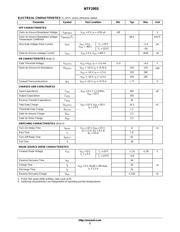
MAXIMUM RATINGS (T
J
= 25°C unless otherwise noted)
Parameter
Symbol Value Unit
Drain−to−Source Voltage V
DSS
−60 V
Gate−to−Source Voltage V
GS
±20 V
Continuous Drain
Current (Note 1)
Steady
State
T
A
= 25°C
I
D
−2.6
A
Current (Note 1) State
T
A
= 85°C −2.0
Power Dissipation
(Note 1)
Steady
State
T
A
= 25°C P
D
2.3
W
Continuous Drain
Current (Note 2)
Steady
State
T
A
= 25°C
I
D
−1.7
A
Current (Note 2) State
T
A
= 85°C −1.3
Power Dissipation
(Note 2)
T
A
= 25°C P
D
1.0 W
Pulsed Drain Current tp = 10 s I
DM
−10.4 A
Operating Junction and Storage Temperature T
J
,
T
STG
−55 to
175
°C
Single Pulse Drain−to−Source Avalanche
Energy (V
DD
= 25 V, V
G
= 10 V, I
PK
= 6.7 A,
L = 10 mH, R
G
= 25 )
EAS 225 mJ
Lead Temperature for Soldering Purposes
(1/8” from case for 10 s)
T
L
260 °C
THERMAL RESISTANCE RATINGS
Parameter Symbol Max Unit
Junction−to−Tab (Drain) − Steady State (Note 2) R
JC
14
°C/W
Junction−to−Ambient − Steady State (Note 1) R
JA
65
Junction−to−Ambient − Steady State (Note 2) R
JA
150
Maximum ratings are those values beyond which device damage can occur.
Maximum ratings applied to the device are individual stress limit values (not
normal operating conditions) and are not valid simultaneously. If these limits are
exceeded, device functional operation is not implied, damage may occur and
reliability may be affected.
1. When surface mounted to an FR4 board using 1 in. pad size
(Cu. area = 1.127 in
2
[1 oz] including traces)
2. When surface mounted to an FR4 board using the minimum recommended
pad size (Cu. area = 0.341 in
2
)
D
S
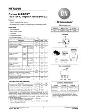
G
P−Channel
http://onsemi.com
−60 V 145 m @ −10 V
R
DS(on)
TYP
−2.6 A
I
D
MAXV
(BR)DSS
1
2
3
4
Device Package Shipping
†
ORDERING INFORMATION
NTF2955T1 SOT−223 1000/Tape & Reel
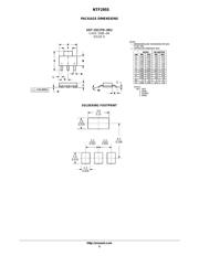
SOT−223
CASE 318E
STYLE 3
LWW
MARKING
DIAGRAM
2955
2955 = Device Code
L = Location Code
WW = Work Week
PIN ASSIGNMENT
321
4
Gate Drain Source
Drain
NTF2955T3 SOT−223 4000/Tape & Reel
†For information on tape and reel specifications,
including part orientation and tape sizes, please
refer to our Tape and Reel Packaging Specification
Brochure, BRD8011/D.
Verzeichnis