


© Semiconductor Components Industries, LLC, 2006
April, 2006 − Rev. 2
1 Publication Order Number:
NTGS4111P/D
NTGS4111P
Power MOSFET
−30 V, −4.7 A, Single P−Channel, TSOP−6
Features
• Leading −30 V Trench Process for Low R
DS(on)
• Low Profile Package Suitable for Portable Applications
• Surface Mount TSOP−6 Package Saves Board Space
• Improved Efficiency for Battery Applications
• Pb−Free Package is Available
Applications
• Battery Management and Switching
• Load Switching
• Battery Protection
MAXIMUM RATINGS (T
J
= 25°C unless otherwise noted)
Rating Symbol Value Unit
Drain−to−Source Voltage V
DSS
−30 V
Gate−to−Source Voltage V
GS
±20 V
Continuous Drain
Current (Note 1)
Stead
y
State
T
A
= 25°C
I
D
−3.7
A
T
A
= 85°C −2.7
t ≤ 5 s T
A
= 25°C −4.7
Power Dissipation
(Note 1)
Steady
State
T
A
= 25°C P
D
1.25
W
t ≤ 5 s 2.0
Continuous Drain
Current (Note 2)
Stead
y
State
T
A
= 25°C
I
D
−2.6
A
T
A
= 85°C −1.9
Power Dissipation
(Note 2)
T
A
= 25°C P
D
0.63 W
Pulsed Drain Current
tp = 10 ms
I
DM
−15 A
Operating Junction and Storage Temperature T
J
,
T
STG
−55 to
150
°C
Source Current (Body Diode) I
S
−1.7 A
Lead Temperature for Soldering Purposes
(1/8″ from case for 10 s)
T
L
260 °C
THERMAL RESISTANCE RATINGS
Rating Symbol Max Unit
Junction−to−Ambient – Steady State (Note 1)
R
q
JA
100
°C/W
Junction−to−Ambient – t ≤ 5 s (Note 1)
R
q
JA
62.5
Junction−to−Ambient – Steady State (Note 2)
R
q
JA
200
Maximum ratings are those values beyond which device damage can occur.
Maximum ratings applied to the device are individual stress limit values (not
normal operating conditions) and are not valid simultaneously. If these limits are
exceeded, device functional operation is not implied, damage may occur and
reliability may be affected.
1. Surface−mounted on FR4 board using 1 in sq pad size
(Cu area = 1.127 in sq [1 oz] including traces).
2. Surface−mounted on FR4 board using the minimum recommended pad size
(Cu area = 0.006 in sq).
3
4
1256
Device Package Shipping
†
ORDERING INFORMATION
NTGS4111PT1 TSOP−6 3000 / Tape & Reel
P−Channel
http://onsemi.com
NTGS4111PT1G TSOP−6
(Pb−Free)
3000 / Tape& Reel
†For information on tape and reel specifications,
including part orientation and tape sizes, please
refer to our Tape and Reel Packaging Specification
s
Brochure, BRD8011/D.
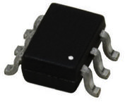
TSOP−6
CASE 318G
STYLE 1
MARKING DIAGRAM &
PIN ASSIGNMENT
1
TG M G
G
TG = Specific Device Code
M
= Date Code*
G = Pb−Free Package
Source
4
Drain
6
Drain
5
3
Gate
1
Drain
2
Drain
(Note: Microdot may be in either location)
*Date Code orientation may vary depending
upon manufacturing location.
−30 V
68 mW @ −4.5 V
38 mW @ −10 V
R
DS(on)
TYP
−4.7 A
I
D
MAX
V
(BR)DSS
Verzeichnis
- ・ Konfiguration des Pinbelegungsdiagramms on Seite 1
- ・ Abmessungen des Paketumrisses on Seite 5
- ・ Paket-Footprint-Pad-Layout on Seite 5
- ・ Teilenummerierungssystem on Seite 1 Seite 5
- ・ Markierungsinformationen on Seite 1
- ・ Technische Daten on Seite 1
- ・ Anwendungsbereich on Seite 1
- ・ Elektrische Spezifikation on Seite 2