


herunterladen
© Semiconductor Components Industries, LLC, 2006
February, 2006 − Rev. 1
1 Publication Order Number:
NTGS4141N/D
NTGS4141N
Power MOSFET
30 V, 7.0 A, Single N−Channel, TSOP−6
Features
• Low R
DS(on)
• Low Gate Charge
• Pb−Free Package is Available
Applications
• Load Switch
• Notebook PC
• Desktop PC
MAXIMUM RATINGS (T
J
= 25°C unless otherwise noted)
Rating Symbol Value Unit
Drain−to−Source Voltage V
DSS
30 V
Gate−to−Source Voltage V
GS
±20 V
Continuous Drain
Current (Note 1)
Steady
State
T
A
= 25°C
I
D
5.0
A
T
A
= 85°C 3.6
t ≤ 10 s T
A
= 25°C 7.0
Power Dissipation
(Note 1)
Steady
State
T
A
= 25°C P
D
1.0
W
t ≤ 10 s 2.0
Continuous Drain
Current (Note 2)
Steady
State
T
A
= 25°C
I
D
3.5
A
T
A
= 85°C 2.5
Power Dissipation
(Note 2)
T
A
= 25°C P
D
0.5 W
Pulsed Drain Current
t
p
= 10 ms
I
DM
21 A
Operating Junction and Storage Temperature T
J
,
T
STG
−55 to
150
°C
Source Current (Body Diode) I
S
2.0 A
Single Pulse Drain−to−Source Avalanche Energy
(V
DD
= 30 V, I
L
= 10.4 A, V
GS
= 10 V,
L = 1.0 mH, R
G
= 25 W)
EAS 54 mJ
Lead Temperature for Soldering Purposes
(1/8″ from case for 10 s)
T
L
260 °C
THERMAL RESISTANCE RATINGS
Rating Symbol Max Unit
Junction−to−Ambient – Steady State (Note 1) R
θ
JA
125
°C/W
Junction−to−Ambient – t ≤ 10 s (Note 1) R
θ
JA
62.5
Junction−to−Ambient – Steady State (Note 2) R
θ
JA
248
1. Surface−mounted on FR4 board using 1 inch sq pad size
(Cu area = 1.127 in sq [1 oz] including traces).
2. Surface−mounted on FR4 board using the minimum recommended pad size
(Cu area = 0.0773 in sq).
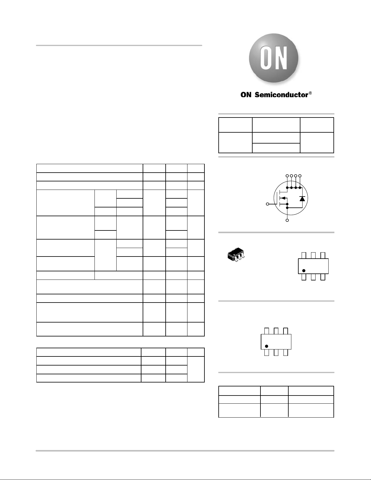
TSOP−6
CASE 318G
STYLE 1
MARKING
DIAGRAM
S4 MG
G
S4 = Device Code
M = Date Code
G = Pb−Free Package
(Note: Microdot may be in either location)
PIN ASSIGNMENT
3
Gate
1
Drain
Source
4
2
Drain
Drain
5
Drain
6
http://onsemi.com
Device Package Shipping
†
ORDERING INFORMATION
NTGS4141NT1 TSOP−6 3000/Tape & Ree
l
NTGS4141NT1G
TSOP−6
(Pb−Free)
3000/Tape & Ree
l
†For information on tape and reel specifications,
including part orientation and tape sizes, please
refer to our Tape and Reel Packaging Specification
Brochure, BRD8011/D.
30 V
30 mW @ 4.5 V
21.5 mW @ 10 V
R
DS(on)
TYP
7.0 A
I
D
MAX
V
(BR)DSS
1256
3
4
Drain
Gate
Source
N−Channel
1
Verzeichnis