


herunterladen
Semiconductor Components Industries, LLC, 2003
August, 2003 − Rev. 0
1 Publication Order Number:
NTJD4001N/D
NTJD4001N
Small Signal MOSFET
30 V, 250 mA, Dual N−Channel, SC−88
Features
• Low Gate Charge for Fast Switching
• Small Footprint − 30% Smaller than TSOP−6
• ESD Protected Gate
• Pb−Free Package for Green Manufacturing (G Suffix)
Applications
• Low Side Load Switch
• Li−Ion Battery Supplied Devices − Cell Phones, PDAs, DSC
• Buck Converters
• Level Shifts
MAXIMUM RATINGS (T
J
= 25°C unless otherwise stated)
Parameter
Symbol Value Units
Drain−to−Source Voltage V
DSS
30 V
Gate−to−Source Voltage V
GS
±20 V
Continuous Drain
Current (Note 1)
Steady
State
T
A
= 25 °C
I
D
250
mA
Current (Note 1) State
T
A
= 85 °C 180
Power Dissipation
(Note 1)
Steady
State
T
A
= 25 °C P
D
272 mW
Pulsed Drain Current t =10 µs I
DM
600 mA
Operating Junction and Storage Temperature T
J
, T
STG
−55 to
150
°C
Source Current (Body Diode) I
S
250 mA
Lead Temperature for Soldering Purposes
(1/8” from case for 10 s)
T
L
260 °C
1. Surface mounted on FR4 board using 1 in sq. pad size
(Cu area = 1.127 in sq. [1 oz] including traces).
Device Package Shipping
ORDERING INFORMATION
NTJD4001NT1 SC−88 3000 Units/Reel
Top View
SC−88 / SOT−363
CASE 419B
STYLE 26
MARKING DIAGRAM
6
1
http://onsemi.com
TE = Device Code
D = Date Code
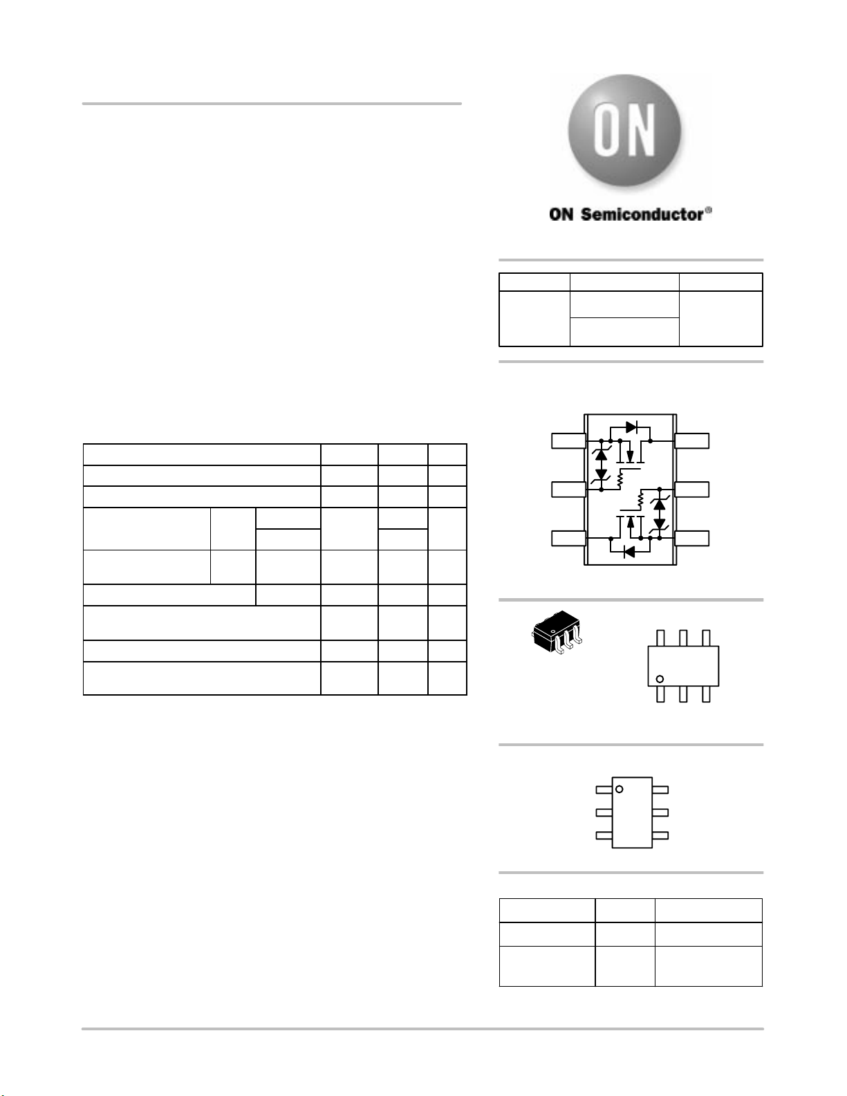
16
Drain−1
Gate−2
Source−2
Source−1
Gate−1
Drain−2
Top View
SOT−363
SC−88 (6 LEADS)
D
1
G
2
S
2
S
1
G
1
6
5
4
1
2
3
V
(BR)DSS
R
DS(on)
TYP I
D
Max
30 V
1.0 @ 4.0 V
1.5 @ 2.5 V
250 mA
NTJD4001NT1G
SC−88
(Pb−Free)
3000 Units/Reel
PIN ASSIGNMENT
TED
D
2
Verzeichnis