


herunterladen
74LVC1G04
Document number: DS32198 Rev. 8 - 2
1 of 14
www.diodes.com
July 2014
© Diodes Incorporated
74LVC1G04
SINGLE INVERTER
Description
The 74LVC1G04 is a single inverter gate with a standard push-pull
output. The device is designed for operation with a power supply
range of 1.65V to 5.5V. The inputs are tolerant to 5.5V allowing this
device to be used in a mixed voltage environment. The device is fully
specified for partial power down applications using I
OFF
. The I
OFF
circuitry disables the output preventing damaging current backflow
when the device is powered down.
The gate performs the positive Boolean function:
A
Y =
Features
• Wide Supply Voltage Range from 1.65 to 5.5V
• ± 24mA Output Drive at 3.3V
• CMOS Low Power Consumption
• I
OFF
Supports Partial-Power-Down Mode Operation
• Inputs Accept Up to 5.5V
• ESD Protection Tested per JESD 22
Exceeds 200-V Machine Model (A115)
Exceeds 2000-V Human Body Model (A114)
Exceeds 1000-V Charged Device Model (C101)
• Latch-Up Exceeds 100mA per JESD 78, Class I
• Range of Package Options
• Direct Interface with TTL Levels
• Totally Lead-Free & Fully RoHS Compliant (Notes 1 & 2)
• Halogen and Antimony Free. “Green” Device (Note 3)
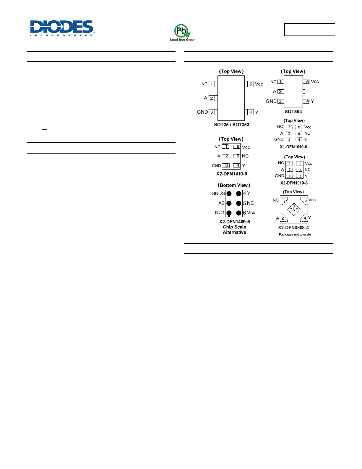
Pin Assignments
Applications
• Voltage Level Shifting
• General Purpose Logic
• Power Down Signal Isolation
• Wide Array of Products Such as.
PCs, Networking, Notebooks, Netbooks, PDAs
Tablet Computers, E-readers
Computer Peripherals, Hard Drives, CD/DVD ROM
TV, DVD, DVR, set top box
Cell Phones, Personal Navigation / GPS
MP3 players ,Cameras, Video Recorders
Notes: 1. No purposely added lead. Fully EU Directive 2002/95/EC (RoHS) & 2011/65/EU (RoHS 2) compliant.
2. See http://www.diodes.com/quality/lead_free.html for more information about Diodes Incorporated’s definitions of Halogen- and Antimony-free, "Green"
and Lead-free.
3. Halogen- and Antimony-free "Green” products are defined as those which contain <900ppm bromine, <900ppm chlorine (<1500ppm total Br + Cl) and
<1000ppm antimony compounds.
Verzeichnis
- ・ Konfiguration des Pinbelegungsdiagramms on Seite 1 Seite 2
- ・ Abmessungen des Paketumrisses on Seite 8 Seite 9 Seite 10
- ・ Paket-Footprint-Pad-Layout on Seite 2 Seite 11 Seite 12 Seite 13
- ・ Teilenummerierungssystem on Seite 2
- ・ Markierungsinformationen on Seite 7
- ・ Typisches Anwendungsschaltbild on Seite 2
- ・ Technische Daten on Seite 3
- ・ Anwendungsbereich on Seite 1
- ・ Elektrische Spezifikation on Seite 4