

herunterladen
© Semiconductor Components Industries, LLC, 2016
October, 2017 − Rev. 2
1 Publication Order Number:
ESD7462/D
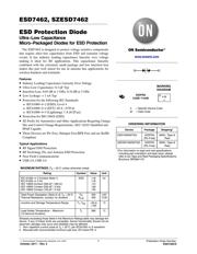
ESD7462, SZESD7462
ESD Protection Diode
Ultra−Low Capacitance
Micro−Packaged Diodes for ESD Protection
The ESD7462 is designed to protect voltage sensitive components
that require ultra−low capacitance from ESD and transient voltage
events. It has industry leading capacitance linearity over voltage
making it ideal for RF applications. This capacitance linearity
combined with the extremely small package and low insertion loss
makes this part well suited for use in antenna line applications for
wireless handsets and terminals.
Features
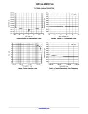
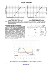
• Industry Leading Capacitance Linearity Over Voltage
• Ultra−Low Capacitance: 0.3 pF Typ
• Insertion Loss: 0.05 dB at 1 GHz; 0.10 dB at 3 GHz
• Low Leakage: < 1 nA Typ
• Protection for the following IEC Standards:
♦ IEC61000−4−2 (ESD): Level 4
♦ IEC61000−4−4 (EFT): 40 A −5/50 ns
♦ IEC61000−4−5 (Lightning): 1 A (8/20 ms)
• Protection for ISO 10605 (ESD)
• SZ Prefix for Automotive and Other Applications Requiring Unique
Site and Control Change Requirements; AEC−Q101 Qualified and
PPAP Capable
• These Devices are Pb−Free, Halogen Free/BFR Free and are RoHS
Compliant
Typical Applications
• RF Signal ESD Protection
• RF Switching, PA, and Antenna ESD Protection
• Near Field Communications
• USB 2.0, USB 3.0
MAXIMUM RATINGS (T
A
= 25°C unless otherwise noted)
Rating Symbol Value Unit
IEC 61000−4−2 Contact (Note 1)
IEC 61000−4−2 Air
ISO 10605 Contact (330 pF / 330 W)
ISO 10605 Contact (330 pF / 2 kW)
ISO 10605 Contact (150 pF / 2 kW)
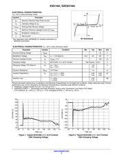
ESD ±18
±18
±13
±29
±30
kV
Total Power Dissipation (Note 2) @ T
A
= 25°C
Thermal Resistance, Junction−to−Ambient
°P
D
°
R
q
JA
300
400
mW
°C/W
Junction and Storage Temperature Range T
J
, T
stg
−55 to
+150
°C
Lead Solder Temperature − Maximum
(10 Second Duration)
T
L
260 °C
Stresses exceeding those listed in the Maximum Ratings table may damage the
device. If any of these limits are exceeded, device functionality should not be
assumed, damage may occur and reliability may be affected.
1. Non−repetitive current pulse at T
A
= 25°C, per IEC61000−4−2 waveform.
2. Mounted with recommended minimum pad size, DC board FR−4
Device Package Shipping
†
ORDERING INFORMATION
www.onsemi.com
†For information on tape and reel specifications,
including part orientation and tape sizes, please
refer to our Tape and Reel Packaging Specifications
Brochure, BRD8011/D.
ESD7462N2T5G X2DFN2
(Pb−Free)
8000 / Tape &
Reel
MARKING
DIAGRAM
4 = Specific Device Code
M = Date Code
X2DFN2
CASE 714AB
4 M
G
SZESD7462N2T5G X2DFN2
(Pb−Free)
8000 / Tape &
Reel
Verzeichnis
- ・ Abmessungen des Paketumrisses on Seite 6
- ・ Teilenummerierungssystem on Seite 1 Seite 6
- ・ Markierungsinformationen on Seite 1 Seite 6
- ・ Blockdiagramm on Seite 5
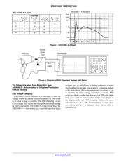
- ・ Typisches Anwendungsschaltbild on Seite 1
- ・ Technische Daten on Seite 1
- ・ Anwendungsbereich on Seite 1
- ・ Elektrische Spezifikation on Seite 2
- ・ Teilenummernliste on Seite 1