
herunterladen
1
SLVA883–April 2017
Submit Documentation Feedback
Copyright © 2017, Texas Instruments Incorporated
Timing of Load Switches
Application Report
SLVA883–April 2017
Timing of Load Switches
NicholasCarley........................................................................................................... PowerSwitches
ABSTRACT
Timing of load switches can vary depending on the operating conditions of the system and feature set of
the device. At a glance, these variations can seem complex; but, when broken down, each operating
condition and feature has a correlation to a change in timing. This application note goes into detail on how
each condition or feature can alter the timing of a load switch so that the variations can be prepared for.
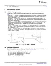
Contents
1 Overview and Main Questions ............................................................................................. 2
1.1 Definition of Timing Parameters .................................................................................. 2
1.2 Alternative Timing Methods ....................................................................................... 2
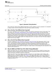
1.3 Why is My Rise Time Different than Expected? ................................................................ 3
1.4 Why is My Fall Time Different than Expected? ................................................................. 3
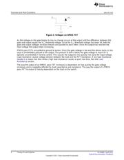
1.5 Why Do NMOS and PMOS Pass FETs Affect Timing Differently?........................................... 3
2 Effect of System Operating Specifications on Timing................................................................... 5
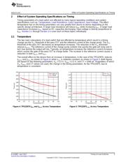
2.1 Temperature......................................................................................................... 5
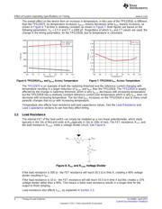
2.2 Load Resistance.................................................................................................... 6
2.3 Load Capacitance .................................................................................................. 7
2.4 Input Voltage ........................................................................................................ 7
3 Effects of Device Features on Timing..................................................................................... 7
3.1 Slew Rate............................................................................................................ 8
3.2 Bias Voltage......................................................................................................... 9
3.3 Quick Output Discharge .......................................................................................... 10
4 Conclusion .................................................................................................................. 11
5 References.................................................................................................................. 11
List of Figures
1 t
DELAY
, t
ON
, t
OFF
, t
RISE
, and t
FALL
Waveforms .................................................................................. 2
2 Alternative Timing Waveform .............................................................................................. 3
3 Voltages on NMOS FET.................................................................................................... 4
4 TPS22975 t
RISE
and t
DELAY
Across Temperature .......................................................................... 5
5 TPS22975
FALL
Across Temperature....................................................................................... 5
6 TPS22918 t
RISE
and t
DELAY
Across Temperature .......................................................................... 6
7 TPS22918 t
FALL
Across Temperature...................................................................................... 6
8 R
FET
and R
LOAD
Voltage Divider............................................................................................. 6
9 TPS22976 t
RISE
vs V
INPUT
..................................................................................................... 7
10 TPS22976 t
DELAY
vs V
INPUT
................................................................................................... 7
11 TPS22958 t
R
vs V
IN
With Changing CT ................................................................................... 8
12 TPS22976 t
DELAY
vs V
INPUT
................................................................................................... 9
13 TPS22976 t
DELAY
vs V
INPUT
................................................................................................... 9
14 TPS22958 t
RISE
vs V
BIAS
...................................................................................................... 9
15 TPS22953 t
RISE
vs V
BIAS
.................................................................................................... 10
16 QOD - Constant Current .................................................................................................. 10