


herunterladen
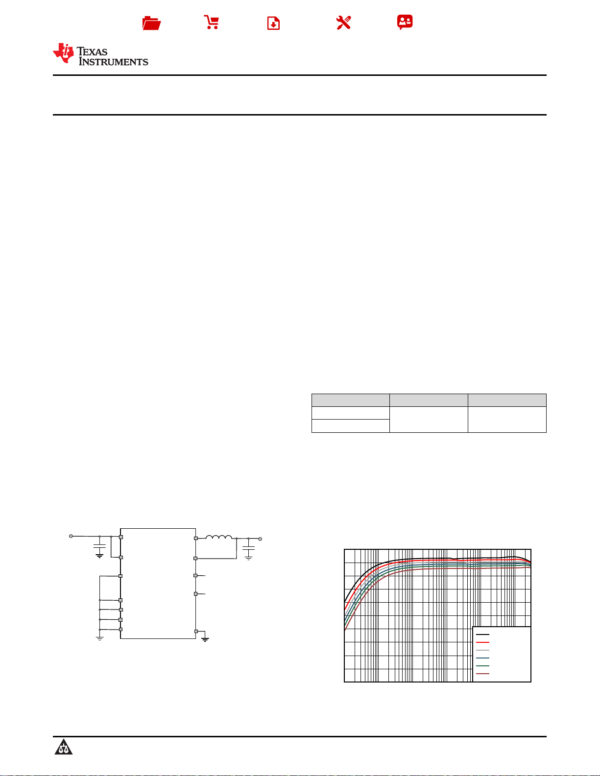
Output Current (A)
Efficiency (%)
0
10
20
30
40
50
60
70
80
90
100
1P 10P 100P 1m 10m 100m
D001
V
IN
= 4.0V
V
IN
= 5.0V
V
IN
= 6.0V
V
IN
= 7.2V
V
IN
= 8.4V
V
IN
= 10.0V
TPS62745
SW
VIN_SW
PG
VIN
VSEL1
VSEL2
VSEL3
VOUT
4.7 Hµ
EN
GND
10 Fµ
10 Fµ
VIN = 3.3 V to 10 V
VOUT = 1.8 V
EN_VIN_SW
VSEL4
CIN
COUT
L
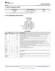
Product
Folder
Sample &
Buy
Technical
Documents
Tools &
Software
Support &
Community
TPS62745
,
TPS627451
SLVSC68A –JUNE 2015–REVISED JUNE 2015
TPS62745 Dual-cell Ultra Low I
Q
Step Down Converter for Low Power Wireless
Applications
1 Features 3 Description
The TPS62745 is a high efficiency ultra low power
1
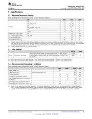
• Input Voltage Range V
IN
from 3.3 V to 10 V
synchronous step down converter optimized for low
• Typical 400 nA Quiescent Current
power wireless applications. It provides a regulated
• Up to 90% efficiency with load currents >15 µA
output voltage consuming only 400-nA quiescent
current. The device operates from two rechargeable
• Up to 300 mA Output Current
Li-Ion batteries, Li-primary battery chemistries such
• RF Friendly DCS-Control™
as Li-SOCl2, Li-SO2, Li-MnO2 or four to six cell
• Low Output Ripple Voltage
alkaline batteries. The input voltage range up to 10 V
allows also operation from a USB port and thin-film
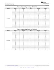
• 16 Selectable Output Voltages from
solar modules. The output voltage is set with four
– 1.8 V to 3.3 V (TPS62745)
VSEL pins between 1.8 V and 3.3 V for TPS62745 or
– 1.3 V to 2.8 V (TPS627451)
1.3 V and 2.8 V for TPS627451. TPS62745 features
• Integrated input voltage switch
low output ripple voltage and low noise with a small
output capacitor. An internal input voltage switch
• Integrated Discharge Function at VOUT
controlled by pin EN_VIN_SW connects the supply
• Open Drain Power Good Output
voltage to pin VIN_SW. The switch is intended to be
• Operates with a Tiny 3.3 µH or 4.7 µH Inductor
used for an external voltage divider, scaling down the
input voltage for an external ADC. The switch is
• Small 3 mm x 2 mm WSON Package
automatically opened when the supply voltage is
below the undervoltage lockout threshold. The
2 Applications
TPS62745 is available in a small 12 pin 3 mm × 2
• Bluetooth® Low Energy, RF4CE, Zigbee
mm WSON package.
• Industrial Metering
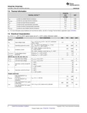
Device Information
(1)
• Energy Harvesting
PART NUMBER PACKAGE BODY SIZE (NOM)
TPS62745
WSON 3 mm x 2 mm
TPS627451
(1) For all available packages, see the orderable addendum at
the end of the datasheet.
4 Typical Application Schematic
spacer
spacer
Efficiency vs Output Current; Vo = 3.3 V
1
An IMPORTANT NOTICE at the end of this data sheet addresses availability, warranty, changes, use in safety-critical applications,
intellectual property matters and other important disclaimers. PRODUCTION DATA.
Verzeichnis
- ・ Konfiguration des Pinbelegungsdiagramms on Seite 3
- ・ Abmessungen des Paketumrisses on Seite 27 Seite 29 Seite 30
- ・ Markierungsinformationen on Seite 27
- ・ Blockdiagramm on Seite 1 Seite 10
- ・ Typisches Anwendungsschaltbild on Seite 1 Seite 13 Seite 21 Seite 23
- ・ Technische Daten on Seite 5 Seite 25
- ・ Anwendungsbereich on Seite 1 Seite 15 Seite 34
- ・ Elektrische Spezifikation on Seite 6 Seite 7