


herunterladen

Application Report
SLVA192 – June 2004
1
Customizing Your TPS6510x/TPS6514x
Jeff Falin PMP Portable Power
ABSTRACT
This application report shows how to use external circuitry to boost the output voltage
capability of the positive and negative charge pumps of the TPS6510x and TPS6514x
triple output power supplies. In addition, the report shows how to use external circuitry to
modify the internally controlled sequencing, implement sequencing delay, and short circuit
protection.
Introduction
When using LCDs with lower liquid crystal cell voltage, the required source voltage from the
main boost converter V
OUT1
is typically 7 V to 8 V. However, the required TFT gate voltage
(VGH) may need to be in the range of 23 V to 24 V. The simplest method to produce VGH is to
quadruple V
OUT1
. In addition, applications like portable DVD players or small-size LCD displays
require a negative voltage, VGL, down to –2 x V
OUT1.
By adding a discrete charge pump
composed of two small external capacitors and a small, SOT-23 or smaller packaged dual
Schottky diode to the charge pump tripled V
OUT3
and inverted V
OUT2
voltages of the TPS6510x/4x
family, the voltages necessary for these applications can easily be realized. The efficiency of the
charge pumps is still acceptable. The approximate efficiency excluding switching and quiescent
current losses of such a charge pump is calculated as shown in Equation 1.
%76
4*5.7
23
*1
3
===
V
V
MVo
Vo
η
with M=Charge pump gain (2, 3, or 4) (1)
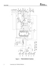
The HPA031EVM for the TPS65140 was modified to implement the circuits described in the
following paragraphs (see Figure 1).