


herunterladen
1 Publication Order Number:
TLV431A/D
Semiconductor Components Industries, LLC, 2004
January, 2004 − Rev. 6
TLV431A, TLV431B
Low Voltage Precision
Adjustable Shunt Regulator
The TLV431A and B series are precision low voltage shunt
regulators that are programmable over a wide voltage range of 1.24 V
to 16 V. The TLV431A series features a guaranteed reference accuracy
of ±1.0% at 25°C and ±2.0% over the entire industrial temperature
range of −40°C to 85°C. For TLV431B series, the accuracy is even
higher, it’s ±0.5% and ±1.0% respectively. These devices exhibit a
sharp low current turn−on characteristic with a low dynamic
impedance of 0.20 over an operating current range of 100 A to
20 mA. This combination of features makes this series an excellent
replacement for zener diodes in numerous applications circuits that
require a precise reference voltage. When combined with an
optocoupler, the TLV431A/B can be used as an error amplifier for
controlling the feedback loop in isolated low output voltage (3.0 V to
3.3 V) switching power supplies. These devices are available in
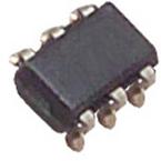
economical TO−92−3 and micro size TSOP−5 and SOT−23−3
packages.
Features
• Programmable Output Voltage Range of 1.24 V to 16 V
• Voltage Reference Tolerance 1.0% for A Series and
0.5% for B Series
• Sharp Low Current Turn−On Characteristic
• Low Dynamic Output Impedance of 0.20 from 100 A to 20 mA
• Wide Operating Current Range of 50 A to 20 mA
• Micro Miniature TSOP−5, SOT−23−3 and TO−92−3 Packages
• Pb−Free Package is Available
Applications
• Low Output Voltage (3.0 V to 3.3 V) Switching Power Supply Error
Amplifier
• Adjustable Voltage or Current Linear and Switching Power Supplies
• Voltage Monitoring
• Current Source and Sink Circuits
• Analog and Digital Circuits Requiring Precision References
• Low Voltage Zener Diode Replacements
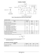
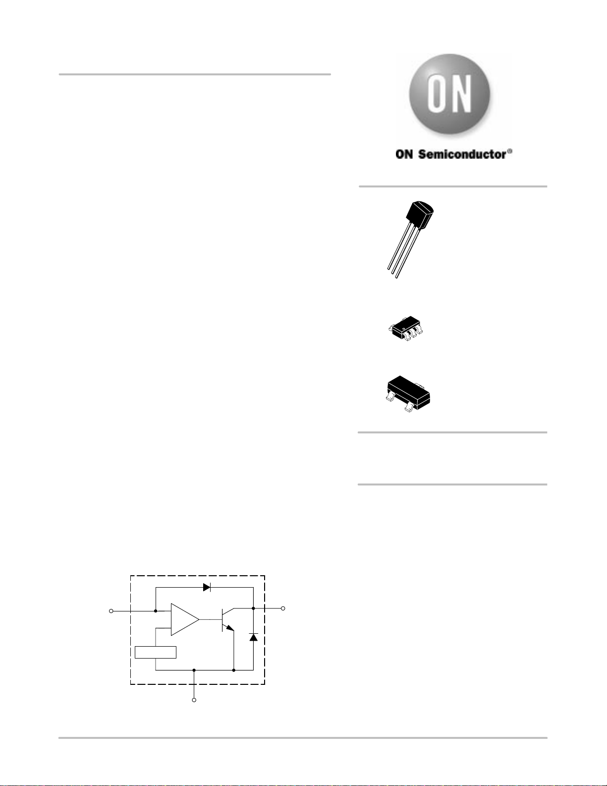
−
+
1.24 V
ref
Reference (R)
Cathode (K)
Anode (A)
Figure 1. Representative Block Diagram
TO−92−3−3
LP SUFFIX
CASE 29
1
2
3
TSOP−5
SN SUFFIX
CASE 483
1
2
3
5
4
SOT−23−3
SN1 SUFFIX
CASE 318
1
2
3
http://onsemi.com
See detailed ordering and shipping information in the package
dimensions section on page 11 of this data sheet.
ORDERING INFORMATION
See general marking information in the device marking
section on page 11 of this data sheet.
DEVICE MARKING INFORMATION
AND PIN CONNECTIONS
Verzeichnis
- ・ Konfiguration des Pinbelegungsdiagramms on Seite 1 Seite 11
- ・ Abmessungen des Paketumrisses on Seite 12 Seite 13 Seite 14
- ・ Paket-Footprint-Pad-Layout on Seite 13 Seite 14
- ・ Teilenummerierungssystem on Seite 1 Seite 11 Seite 14
- ・ Markierungsinformationen on Seite 1 Seite 11
- ・ Blockdiagramm on Seite 1 Seite 2
- ・ Typisches Anwendungsschaltbild on Seite 7
- ・ Technische Daten on Seite 11
- ・ Anwendungsbereich on Seite 1 Seite 7
- ・ Elektrische Spezifikation on Seite 3