

herunterladen

Design Guidelines
For 78P235x
E4/STM1e LIUs
APPLICATION NOTE
Page 1 of 15 2008 Teridian Semiconductor Corp. Rev 2.1
A Maxim Integrated Products Brand
AUGUST 2008
APPLICATION NOTE CONTENTS
Introduction to TERIDIAN 78P235x LIUs
Layout Guidelines
Recommended I/O Terminations
Transformers
Supplemental Surge Protection
Return Loss Matching Circuit (optional)
Coaxial Connectors
Crystal Oscillator Requirements
Thermally Enhanced LQFPs
E4 Reference Design
Sample Jitter and Pulse Mask Test Results
APPLICABLE DEVICES
78P2352 Dual Channel LIU
78P2351 Single Channel LIU
78P2351R Small form factor LIU
INTRODUCTION TO TERIDIAN 78P235x LIUs
The TERIDIAN 78P235x STM1e/E4 Line Interface Units (LIU) ICs are TERIDIAN’s second-generation design.
Next generation design architectures and techniques are used to provide system designers with enhanced
functionality, performance and improved noise immunity.
On the receiver side, one such technique is the use of a digital PLL, rather than the traditional analog PLL. Note
the absence of the external loop filter capacitor. Thanks to the digital PLL, this is now provided on chip. The
removal of the pin and external connection for this critical node eliminates EMI, a noise injection port, and
significantly improves the noise immunity. Additionally, since the loop damping is controlled on chip and is digital,
the 0.1dB jitter peaking specification is now guaranteed by the digital loop filter.
Traditionally, an external 1% resistor is used to set the transmitter amplitude, and sometimes used in setting
internal biasing. Thus, the pin can be a source of EMI pickup directly into critical blocks of the device. On this
generation design, this external resistor and pin have been removed and placed internally, thus completely
eliminating the potential for EMI interference.
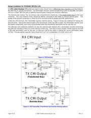
LAYOUT AND I/O TERMINATION GUIDELINES
When designing an analog interface for error-free performance, there are several important factors to consider.
This document provides a few recommendations that can help alleviate unwanted noise due to sub-optimal board
layout around the LIU. It also provides general guidelines for meeting the stringent return loss and CMI transmit
pulse shape requirements, both of which are largely dependant on PCB design and layout.
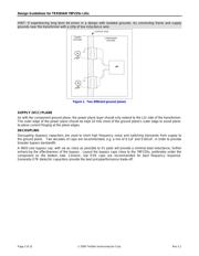
GROUND PLANE
A common system grounding approach is to use a different ground at the coax connectors for safety isolation and
improved electromagnetic compatibility. In this implementation, the coax connector shield is directly connected to
frame or chassis ground. The component ground is an isolated plane that connects directly to the negative supply
pins of active components. These grounds are isolated from each other by placing a strip of area, which is void of
copper, in the ground plane underneath the primary of the transformers as shown in Figure 1 below.
The chassis/frame ground plane is directly connected to the equipment chassis, which connects to the facilities
Earth ground structure. Reference ITU-T recommendation K.27 for more information on grounding
recommendations.