

herunterladen
Quad, 10-Bit nanoDAC
®
with 2 ppm/°C Reference, SPI Interface
Data Sheet
AD5317R
Rev. A Document Feedback
Information furnished by Analog Devices is believed to be accurate and reliable. However, no
responsibility is assumed by Analog Devices for its use, nor for any infringements of patents or other
rights of third parties that may result from its use. Specifications subject to change without notice. No
license is granted by implication or otherwise under any patent or patent rights of Analog Devices.
Trademarks and registered trademarks are the property of their respective owners.
One Technology Way, P.O. Box 9106, Norwood, MA 02062-9106, U.S.A.
Tel: 781.329.4700 ©2012–2014 Analog Devices, Inc. All rights reserved.
Technical Support www.analog.com
FEATURES
Low drift 2.5 V reference: 2 ppm/°C typical
Tiny package: 3 mm × 3 mm, 16-lead LFCSP
Total unadjusted error (TUE): ±0.1% of FSR maximum
Offset error: ±1.5 mV maximum
Gain error: ±0.1% of FSR maximum
High drive capability: 20 mA, 0.5 V from supply rails
User selectable gain of 1 or 2 (GAIN pin)
Reset to zero scale or midscale (RSTSEL pin)
1.8 V logic compatibility
50 MHz SPI with readback or daisy chain
Low glitch: 0.5 nV-sec
Robust 4 kV HBM and 1.5 kV FICDM ESD rating
Low power: 3.3 mW at 3 V
2.7 V to 5.5 V power supply
−40°C to +105°C temperature range
APPLICATIONS
Digital gain and offset adjustment
Programmable attenuators
Industrial automation
Data acquisition systems
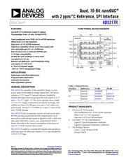
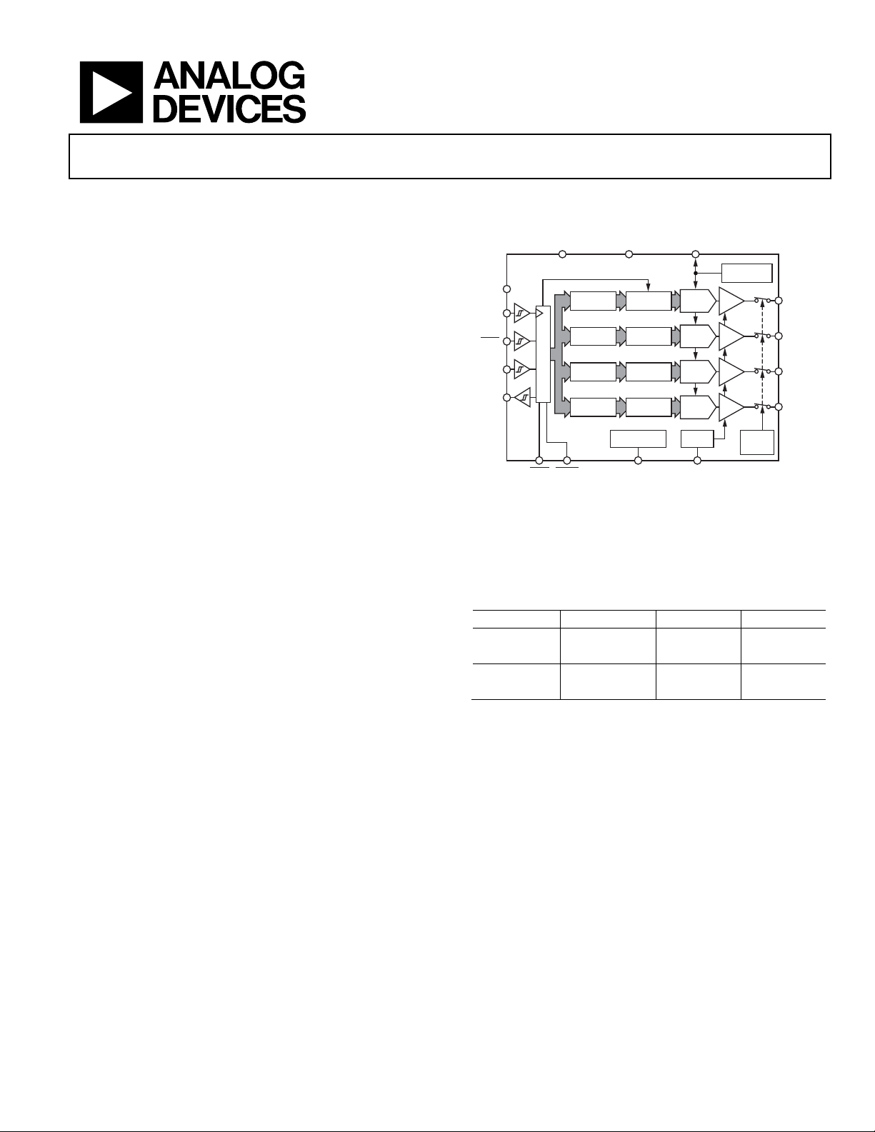
FUNCTIONAL BLOCK DIAGRAM
Figure 1.
GENERAL DESCRIPTION
The AD5317R, a member of the nanoDAC® family, is a low
power, quad, 10-bit buffered voltage output DAC. The device
includes a 2.5 V, 2 ppm/°C internal reference (enabled by
default) and a gain select pin giving a full-scale output of 2.5 V
(gain = 1) or 5 V (gain = 2). The device operates from a single
2.7 V to 5.5 V supply, is guaranteed monotonic by design, and
exhibits less than 0.1% FSR gain error and 1.5 mV offset error
performance. The device is available in a 3 mm × 3 mm LFCSP
and a TSSOP package.
The AD5317R also incorporates a power-on reset circuit and a
RSTSEL pin that ensures that the DAC outputs power up to
zero scale or midscale and remain at that level until a valid write
takes place. Each part contains a per-channel power-down
feature that reduces the current consumption of the device to
4 µA at 3 V while in power-down mode.
The AD5317R employs a versatile SPI interface that operates at
clock rates up to 50 MHz and contains a V
LOGIC
pin intended for
1.8 V/3 V/5 V logic.
Table 1. Related Devices
Interface Reference 12-Bit 10-Bit
SPI Internal AD5684R
External AD5684 AD5317
1
I
2
C Internal AD5694R AD5316R
External AD5694 AD5316
1
The AD5317 and AD5317R are not pin-to-pin or software compatible.
PRODUCT HIGHLIGHTS
1. Precision DC Performance.
Total unadjusted error: ±0.1% of FSR maximum
Offset error: ±1.5 mV maximum
Gain error: ±0.1% of FSR maximum
2. Low Drift 2.5 V On-Chip Reference.
2 ppm/°C typical temperature coefficient
5 ppm/°C maximum temperature coefficient
3. Two Package Options.
3 mm × 3 mm, 16-lead LFCSP
16-lead TSSOP
SCLK
V
LOGIC
SYNC
SDIN
SDO
INPUT
REGISTER
DAC
REGISTER
STRING
DAC A
BUFFER
V
OUT
A
INPUT
REGISTER
DAC
REGISTER
STRING
DAC B
BUFFER
V
OUT
B
INPUT
REGISTER
DAC
REGISTER
STRING
DAC C
BUFFER
V
OUT
C
INPUT
REGISTER
DAC
REGISTER
STRING
DAC D
BUFFER
V
OUT
D
V
REF
GNDV
DD
2.5V
REFERENCE
POWER-
DOWN
LOGIC
POWER-ON
RESET
GAIN
×1/×2
INTERFACE LOGIC
RSTSEL GAINLDAC
RESET
AD5317R
10800-001
Verzeichnis
- ・ Konfiguration des Pinbelegungsdiagramms on Seite 11 Seite 29
- ・ Abmessungen des Paketumrisses on Seite 29
- ・ Teilenummerierungssystem on Seite 29
- ・ Blockdiagramm on Seite 1 Seite 20
- ・ Schweißen Temperatur on Seite 10
- ・ Beschreibung der Funktionen on Seite 1 Seite 11 Seite 29
- ・ Technische Daten on Seite 1 Seite 4 Seite 8 Seite 10
- ・ Anwendungsbereich on Seite 1 Seite 27
- ・ Elektrische Spezifikation on Seite 12