

herunterladen

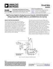
Circuit Note
CN-0079
Circuit Designs Using Analog Devices Products
Apply these product pairings quickly and with confidence.
For more information and/or support call 1-800-AnalogD
(1-800-262-5643) or visit www.analog.com/circuit.
Devices Connected/Referenced
AD5542 16-Bit Serial Input, Voltage Output DAC
ADR421
Precision 2.5 V Voltage Reference
AD8628
Auto-Zero Operational Amplifier
High Precision Digital-to-Analog Conversion Using the 16-Bit AD5542/AD5541
Voltage Output DAC, ADR421 Reference, and AD8628 Auto-Zero Op Amp
Rev. 0
“Circuits from the Lab” from Analog Devices have been designed and built by Analog Devices
engineers. Standard engineering practices have been employed in the design and construction of
each circuit, and their function and performance have been tested and verified in a lab environment
at room temperature. However, you are solely responsible for testing the circuit and determining its
suitability and applicability for your use and application. Accordingly, in no event shall Analog
Devices be liable for direct, indirect, special, incidental, consequential or punitive damages due to
any cause whatsoever connected to the use of any “Circuit from the Lab”. (Continued on last page)
One Technology Way, P.O. Box 9106, Norwood, MA 02062-9106, U.S.A.
Tel: 781.329.4700
www.analog.com
Fax: 781.461.3113 ©2009 Analog Devices, Inc. All rights reserved.
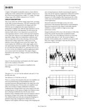
CIRCUIT FUNCTION AND BENEFITS
This circuit provides precision data conversion using the
AD5542 voltage output DAC together with the ADR421BRZ
voltage reference and the AD8628 auto-zero op amp as the
reference buffer. The AD8628 reference buffer provide benefits
previously found only in expensive auto-zeroing or chopper-
stabilized amplifiers. Using Analog Devices, Inc., circuit
topology, these zero-drift amplifiers combine low cost with high
accuracy and low noise. No external capacitor is required, and
the digital switching noise associated with most chopper-
stabilized amplifiers is greatly reduced, thereby making this the
optimum choice for reference buffering.
This circuit provides precision, low power, voltage output,
digital-to-analog conversion. The AD5542 can be operated in
either the buffered or unbuffered mode. The application and its
requirements on settling time, input impedance, noise, etc.,
determine which mode of operation is best. The selection of the
output buffer amplifier can be tailored to suit either dc
precision or fast settling time. Where the DAC is required to
drive a load less than 60 kΩ, an output buffer will be required.
The output impedance of the DAC is constant and code
independent, but to minimize gain errors the input impedance
of the output amplifier should be as high as possible. The output
amplifier should also have a 3 dB bandwidth of 1 MHz or
greater. The output amplifier adds another time constant to the
system, thereby increasing the settling time of the final output.
08312-001
OUT
REFSREFF
GND
TRIM
INV
*
*OUTPUT AMPLIFIER SHOULD
BE CHOSEN TO SUIT
APPLICATION NEEDS.
R
FB
R
INV
DGND AGNDF
V
DD
V
OUT
V
IN
DIN
SCLK
LDAC
CS
AD5541/AD5542
AGNDS
+
0.1µF
0.1µF1µF
0.1µF
10µF
+2.5V
+5V
SERIAL
INTERFACE
RFB
6
5
4
2
+5V
AD8628
ADR421
Figure 1. Precision DAC Configuration (Simplified Schematic)