

herunterladen
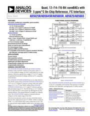
Quad, 12-/14-/16-Bit nanoDACs with
5 ppm/°C On-Chip Reference, I
2
C Interface
Data Sheet
AD5625R/AD5645R/AD5665R, AD5625/AD5665
Rev. D Document Feedback
Information furnished by Analog Devices is believed to be accurate and reliable. However, no
responsibility is assumed by Analog Devices for its use, nor for any infringements of patents or other
rights of third parties that may result from its use. Specifications subject to change without notice. No
license is granted by implication or otherwise under any patent or patent rights of Analog Devices.
Trademarks and registered trademarks are the property of their respective owners.
One Technology Way, P.O. Box 9106, Norwood, MA 02062-9106, U.S.A.
Tel: 781.329.4700 ©2007-2015 Analog Devices, Inc. All rights reserved.
Technical Support www.analog.com
FEATURES
Low power, smallest pin-compatible, quad nanoDACs
AD5625R/AD5645R/AD5665R
12-/14-/16-bit nanoDACs
On-chip, 2.5 V, 5 ppm/°C reference in TSSOP
On-chip, 2.5 V, 10 ppm/°C reference in LFCSP
On-chip, 1.25 V, 10 ppm/°C reference in LFCSP
AD5625/AD5665
12-/16-bit nanoDACs
External reference only
3 mm × 3 mm, 10-lead LFCSP; 14-lead TSSOP; and
1.665 mm × 2.245 mm, 12-ball WLCSP
2.7 V to 5.5 V power supply
Guaranteed monotonic by design
Power-on reset to zero scale/midscale
Per channel power-down
Hardware
LDAC
and
CLR
functions
I
2
C-compatible serial interface supports standard (100 kHz),
fast (400 kHz), and high speed (3.4 MHz) modes
APPLICATIONS
Process control
Data acquisition systems
Portable battery-powered instruments
Digital gain and offset adjustment
Programmable voltage and current sources
Programmable attenuators
GENERAL DESCRIPTION
The AD5625R/AD5645R/AD5665R and AD5625/AD5665
members of the nanoDAC® family are low power, quad, 12-/
14-/16-bit, buffered voltage-out DACs with/without an on-chip
reference. All devices operate from a single 2.7 V to 5.5 V supply,
are guaranteed monotonic by design, and have an I
2
C-compatible
serial interface.
The AD5625R/AD5645R/AD5665R have an on-chip reference.
The LFCSP versions of the AD5625R/AD5645R/AD5665R have a
1.25 V or 2.5 V, 10 ppm/°C reference, giving a full-scale output
range of 2.5 V or 5 V; the TSSOP versions of the AD5625R/
AD5645R/AD5665R have a 2.5 V, 5 ppm/°C reference, giving a
full-scale output range of 5 V. The WLCSP has a 1.25 V reference.
The on-chip reference is off at power-up, allowing the use of an
external reference. The internal reference is enabled via a software
write. The AD5625/AD5665 require an external reference
voltage to set the output range of the DAC.
The device incorporates a power-on reset circuit that ensures
that the DAC output powers up to 0 V (POR = GND) or midscale
(POR = V
DD
) and remains there until a valid write occurs. The
on-chip precision output amplifier enables rail-to-rail output swing.
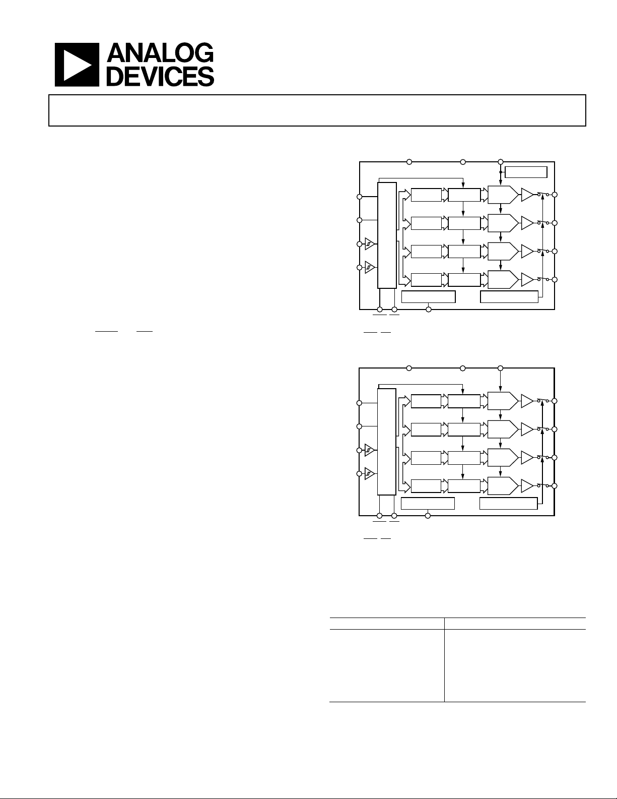
FUNCTIONAL BLOCK DIAGRAMS
Figure 1. AD5625R/AD5645R/AD5665R
Figure 2. AD5625/AD5665
The AD5625R/AD5645R/AD5665R and AD5625/AD5665 use a
2-wire I
2
C-compatible serial interface that operates in standard
(100 kHz), fast (400 kHz), and high speed (3.4 MHz) modes.
Table 1. Related Devices
Device Number
Description
AD5025/AD5045/AD5065 Dual 12-/14-/16-bit DACs
AD5624R/AD5644R/AD5664R,
AD5624/AD5664
Quad SPI 12-/14-/16-bit DACs,
with/without internal reference
AD5627R/AD5647R/AD5667R,
AD5627/AD5667
Dual I
2
C 12-/14-/16-bit DACs,
with/without internal reference
AD5666 Quad SPI 16-bit DAC with internal
reference
INTERFACE
LOGIC
SDA
SCL
ADDR1
ADDR2
V
DD
GND
1.25V/2.5V REF
V
REFIN
/V
REFOUT
AD5625R/AD5645R/AD5665R
INPUT
REGISTER
DAC
REGISTER
STRING
DAC A
V
OUT
A
BUFFER
LDAC CLR POR
INPUT
REGISTER
DAC
REGISTER
STRING
DAC B
V
OUT
B
BUFFER
INPUT
REGISTER
DAC
REGISTER
STRING
DAC C
V
OUT
C
BUFFER
INPUT
REGISTER
DAC
REGISTER
STRING
DAC D
V
OUT
D
BUFFER
NOTES
1. THE FOLLOWING PINS ARE AVAILABLE ONLY ON 14-LEAD PACKAGE:
ADDR2, LDAC, CLR, POR.
06341-001
POWER-ON RESET POWER-DOWN LOGIC
06341-002
INTERFACE
LOGIC
SDA
SCL
ADDR1
ADDR2
V
DD
GND
V
REFIN
AD5625/AD5665
INPUT
REGISTER
DAC
REGISTER
STRING
DAC A
V
OUT
A
BUFFER
LDAC CLR POR
INPUT
REGISTER
DAC
REGISTER
STRING
DAC B
V
OUT
B
BUFFER
INPUT
REGISTER
DAC
REGISTER
STRING
DAC C
V
OUT
C
BUFFER
INPUT
REGISTER
DAC
REGISTER
STRING
DAC D
V
OUT
D
BUFFER
NOTES
1. THE FOLLOWING PINS ARE AVAILABLE ONLY ON 14-LEAD PACKAGE:
ADDR2, LDAC, CLR, POR.
POWER-ON RESET POWER-DOWN LOGIC
Verzeichnis
- ・ Konfiguration des Pinbelegungsdiagramms on Seite 11 Seite 12 Seite 24 Seite 33
- ・ Abmessungen des Paketumrisses on Seite 33
- ・ Teilenummerierungssystem on Seite 23 Seite 24 Seite 26 Seite 35
- ・ Blockdiagramm on Seite 1
- ・ Schweißen Temperatur on Seite 10
- ・ Beschreibung der Funktionen on Seite 1 Seite 11 Seite 12 Seite 33
- ・ Technische Daten on Seite 1 Seite 3 Seite 5 Seite 8 Seite 10
- ・ Anwendungsbereich on Seite 1 Seite 32
- ・ Elektrische Spezifikation on Seite 13