
herunterladen
Evaluation Board User Guide
UG-203
One Technology Way • P. O. Box 9106 • Norwood, MA 02062-9106, U.S.A. • Tel: 781.329.4700 • Fax: 781.461.3113 • www.analog.com
Evaluating the AD9550 Integer-N Clock Translator
PLEASE SEE THE LAST PAGE FOR AN IMPORTANT
WARNING AND LEGAL TERMS AND CONDITIONS.
Rev. 0 | Page 1 of 8
FEATURES
Converts preset standard input frequencies to standard
output frequencies
Input frequencies from 8 kHz to 200 MHz
Output frequencies up to 810 MHz LVPECL and LVDS
(200 MHz CMOS)
Preset pin-programmable frequency translation ratios
On-chip VCO
Single-ended CMOS reference input
2 output clocks (independently programmable as LVDS,
LVPECL, or CMOS)
Single supply (3.3 V)
Very low power: <450 mW (under most conditions)
Small package size: 5 mm × 5 mm
Exceeds Telcordia GR-253-CORE jitter generation, transfer
and tolerance specifications
APPLICATIONS
Cost effective replacement of high frequency VCXO, OCXO,
and SAW resonators
Flexible frequency translation for wireline applications such
as Ethernet, T1/E1, SONET/SDH, GPON, xDSL
Wireless infrastructure
Test and measurement (including handheld devices)
GENERAL DESCRIPTION
This user guide describes the hardware of the AD9550 eval-
uation board. The AD9550 evaluation board is a compact,
easy-to-use platform for evaluating all features of the AD9550
integer-N clock translator.
The AD9550 is a phase-locked loop (PLL) based clock trans-
lator designed to address the needs of wireline communication
and base station applications. The device employs an integer-N
PLL to accommodate the applicable frequency translation
requirements. It accepts a single-ended input reference signal
at the REF input.
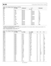
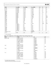
The AD9550 is pin programmable, providing a matrix of
standard input/output frequency translations from a list of
15 possible input frequencies to a list of 52 possible output
frequency pairs (OUT1 and OUT2).
The AD9550 output is compatible with LVPECL, LVDS, or
single-ended CMOS logic levels, although the AD9550 is
implemented in a strictly CMOS process.
The AD9550 operates over the extended industrial temperature
range of −40°C to +85°C.
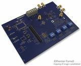
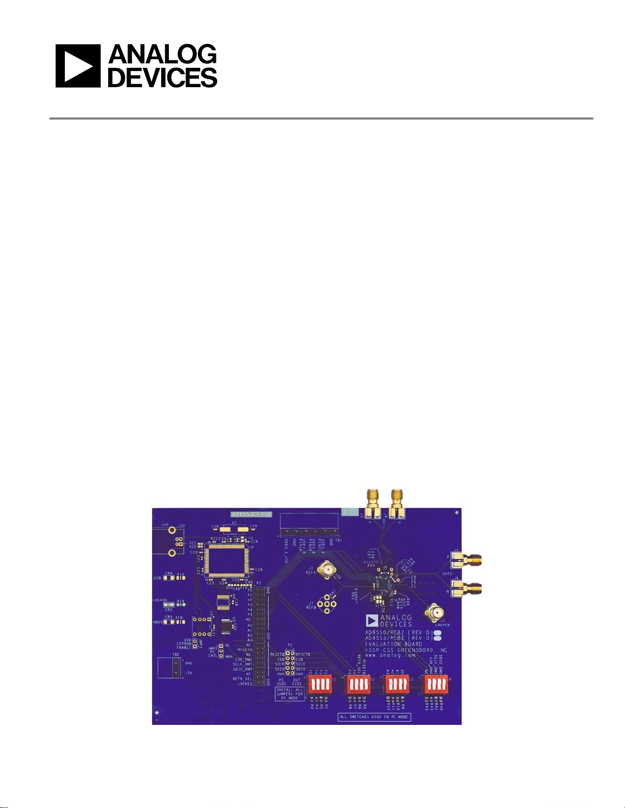
DIGITAL PICTURE OF THE AD9550 EVALUATION BOARD
09452-001
Figure 1. AD9550 Evaluation Board
Verzeichnis