


herunterladen
Evaluation Board User Guide
UG-377
One Technology Way • P. O. Box 9106 • Norwood, MA 02062-9106, U.S.A. • Te l: 781.329.4700 • Fax: 781.461.3113 • www.analog.com
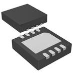
Evaluation Board for the ADA4830-1, High Speed Difference Amplifier
Offered in 8-Lead LFCSP
PLEASE SEE THE LAST PAGE FOR AN IMPORTANT
WARNING AND LEGAL TERMS AND CONDITIONS.
Rev. 0 | Page 1 of 8
FEATURES
Enables quick breadboarding/prototyping
Edge-mounted SMA connector provisions
Easy connection to test equipment and other circuits
GENERAL DESCRIPTION
The ADA4830-1BCP-EBZ evaluation board makes it easy for
designers to quickly observe the performance of the ADA4830-1
difference amplifier in real-world applications. Input signals are
applied through SMA jacks (INP, INN), and the output is taken
from SMA Jack VOUT. Power is applied through the red +VS
pin. The black GND pin should be grounded.
The ADA4830-1BCP-EBZ inputs can be driven by either a
balanced (differential) or unbalanced (single-ended) source. For
unbalanced signals, connect the unused input (INN) to ground
at the signal source. The evaluation board is shipped with a
75 Ω differential input termination at R5. The ADA4830-1BCP-
EBZ board is configured with a 75 Ω series resistor, R6,
installed at the output. This can be changed to match the actual
load impedance. The VREF pin at the upper left of the board
can be used to set the output bias voltage. It is internally biased
to +VS/2 when this pin is floating. Resistors R1 and R2 are
provided as an option to force a new bias level at VREF.
The ADA4830-1 can be powered down (disabled) by grounding
the ENA pin at the top right of the evaluation board. On the
evaluation board, this pin can be pulled up to +VS through
Resistor R3 or left floating for normal operation.
In normal operation, the open-drain short-to-battery output
flag (STB) is held at a logic high, connected to +VS through
Resistor R8. During a short-to-battery condition (9.5 V to 18 V
on either input), it is driven to a logic low state. The STB pin
(lower right of the evaluation board) can be used to monitor the
short-to-battery indicator function.
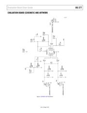
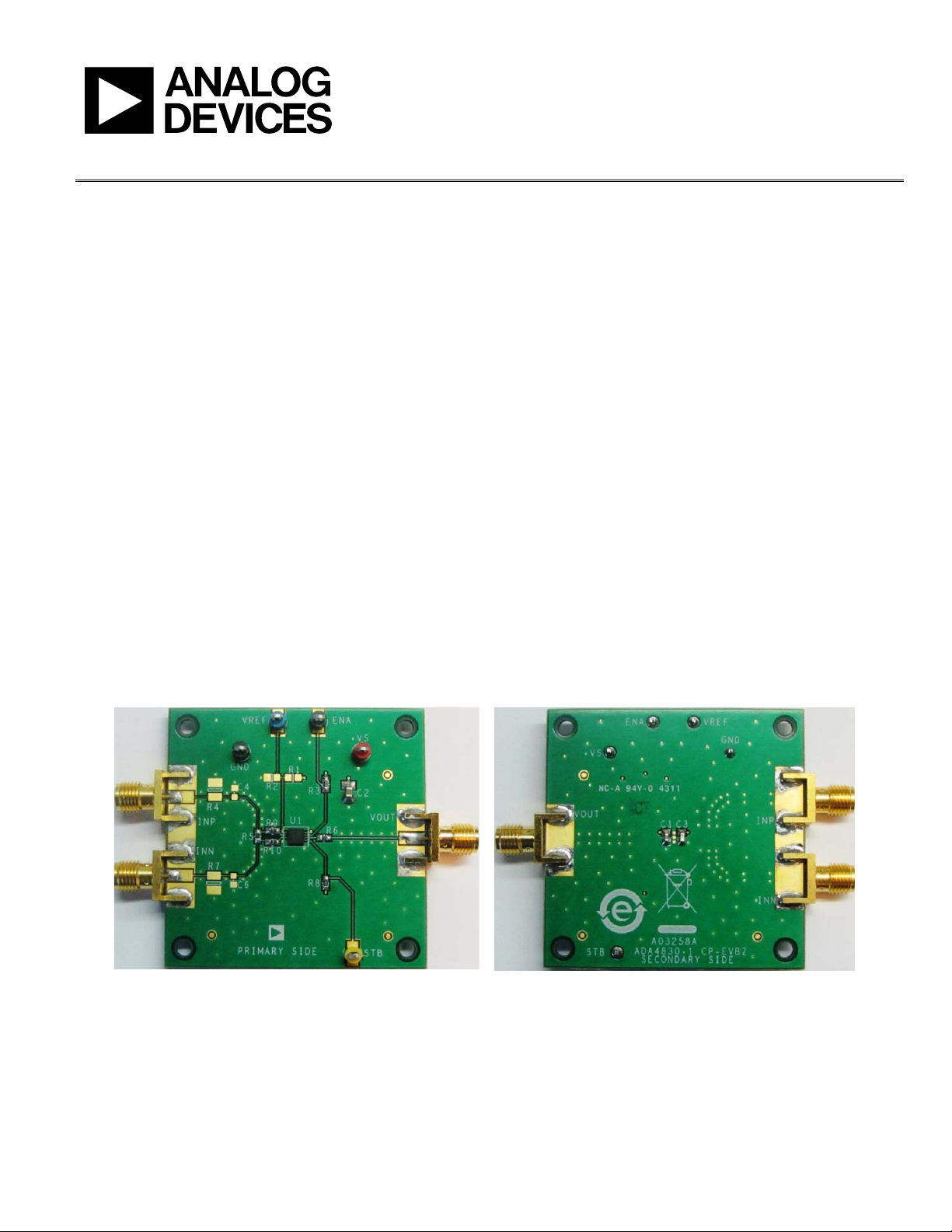
Figure 1 shows the bare evaluation board, component side and
circuit side. Figure 2 shows the evaluation board schematic. The
PCB layout pattern for the PCB is shown in Figure 3 and Figure 4.
DIGITAL PICTURE OF EVALUATION BOARD
Figure 1. ADA4830-1BCP-EBZ Component Side (Primary) and Circuit Side (Secondary) of PCB
10543-001
SECONDARY SIDEPRIMARY SIDE
NOTES
1. THE
E
VALUATION BOARD SILKSCREEN PART NUMBER LABELING ON YOUR BOARD MAY BE DIFFERENT
FROM WHAT IS SHOWN HERE.
Verzeichnis