
herunterladen
AN-772
APPLICATION NOTE
One Technology Way • P.O. Box 9106 • Norwood, MA 02062-9106 • Tel: 781/329-4700 • Fax: 781/461-3113 • www.analog.com
TABLE OF CONTENTS
Introduction ....................................................................... 1
Description ......................................................................... 1
Board Design Considerations ...........................................
2
Assembly Considerations .................................................
5
Rework ................................................................................ 7
Thermal Performance ........................................................ 9
Electrical Characteristics ..................................................
10
Solder Joint Reliability ....................................................
12
References ........................................................................ 14
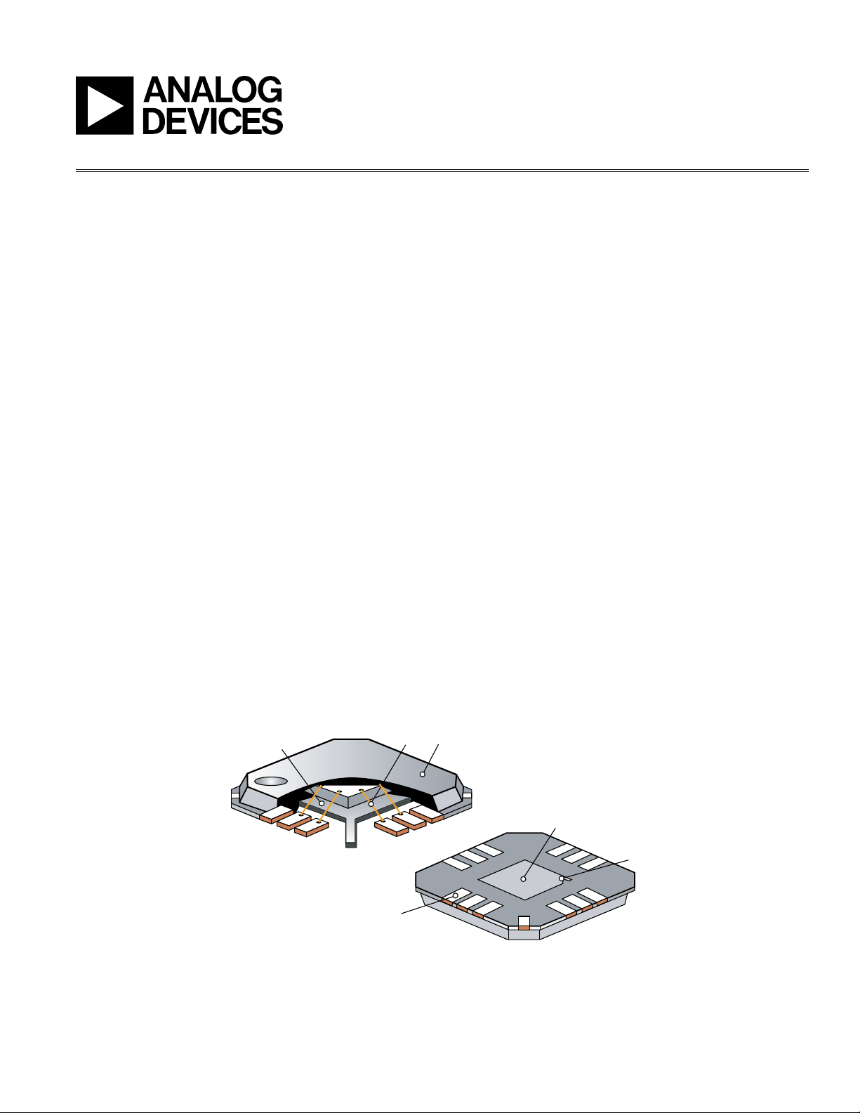
A Design and Manufacturing Guide for the Lead Frame Chip Scale Package (LFCSP)
by Gary Griffin
INTRODUCTION
This application note provides design and manu-
facturing guidance in the use of the lead frame chip
scale package (LFCSP). The LFCSP is compliant with
JEDEC MO220 and MO229 outlines.
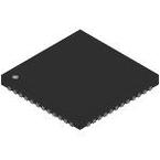
DESCRIPTION
The LFCSP is a near chip scale package (CSP), a plastic
encapsulated wire bond package with a copper lead
frame substrate in a leadless package format.
Perimeter input/output pads are located on the outside
edges of the package. Electrical contact to the printed
circuit board (PCB) is made by soldering the perimeter
pads and exposed paddle on the bottom surface of the
package to the PCB. Heat is efficiently conducted from
the package by soldering the exposed thermal paddle
(see Figure 1) to the PCB. Stable electrical ground
connections are provided through down bonds and
through conductive die attach material. Wire bonding
is provided using gold wires (see Figure 2). Perimeter
and thermal pad finish is plated as Sn/Pb solder or
100% Sn. Packaging is in tape and reel or trays.
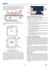
DIE PAD
GOLD
WIRE
MOLDING
COMPOUND
EXPOSED
THERMAL PADDLE
PIN 1
PERIMETER
I/O PADS
(LEADS)
Figure 1. Isometric Cut Away View of the LFCSP
REV. 0
Verzeichnis