

herunterladen

User's Guide
SLAU333A–March 2011–Revised June 2013
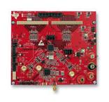
ADS42xx EVM
This is the user’s guide for the ADS42xx EVM Rev B (EVM). The ADS42xx (dual channel, 12-bit and 14-
bit, up to 250 MSPS) is a dual analog-to-digital converter family. This EVM is specifically suited for
interfacing with TI’s TSW1400 EVM to capture and display waveforms from the ADC. The EVM schematic,
BOM, and layout files can be found in the design package in the ADS42xx EVM product folder on
www.ti.com.
Contents
1 Software Control ............................................................................................................ 2
1.1 Installation Instructions ............................................................................................ 2
1.2 Software Operation ................................................................................................ 2
2 Basic Test Procedure ....................................................................................................... 5
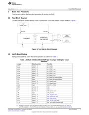
2.1 Test Block Diagram ................................................................................................ 5
2.2 Verify Board Set-up ................................................................................................ 5
2.3 Test Set-up Connections .......................................................................................... 6
2.4 TSW1400 Quick start Operation ................................................................................. 6
2.5 ADS42xx Test Procedure ......................................................................................... 8
3 Optional Configurations .................................................................................................... 9
3.1 THS4509 Input Op-Amp Configuration .......................................................................... 9
3.2 On-Board CDCE72010 Clock .................................................................................... 9
3.3 Parallel CMOS Output ........................................................................................... 10
List of Figures
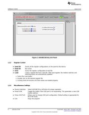
1 ADS42xx/58C28 GUI Front Panel ........................................................................................ 3
2 ADS58C28-Only GUI Panel ............................................................................................... 4
3 Test Set-Up Block Diagram................................................................................................ 5
4 FFT Plot: 160-MHz Clock, 15.5-MHz Input.............................................................................. 8
List of Tables
1 Default ADS42xx/58C28 EVM Rev B Jumper Setting for Serial Interface .......................................... 5
2 Parallel Interface with Pin Control of the ADS42xx/58C28 EVM Rev B Jumper Setting .......................... 6
3 Jumper Setting for Transformer-Coupled or OPA-Driven Input ...................................................... 9
4 Jumper Setting for Transformer-Coupled or CDCE72010 Input ..................................................... 9
5 Jumper and Component Setting for DDR LVDS Output and Parallel CMOS Output ............................ 10
Windows is a registered trademark of Microsoft Corporation.
1
SLAU333A–March 2011–Revised June 2013 ADS42xx EVM
Submit Documentation Feedback
Copyright © 2011–2013, Texas Instruments Incorporated
Verzeichnis
- ・ Blockdiagramm on Seite 5
- ・ Anwendungsbereich on Seite 14 Seite 15