


herunterladen
ADS5102
ADS5103
SLAS351B – OCTOBER 2001 – REVISED DECEMBER 2001
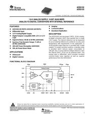
1.8-V ANALOG SUPPLY, 10-BIT, 65/40 MSPS
ANALOG-TO-DIGITAL CONVERTERS WITH INTERNAL REFERENCE
1
www.ti.com
FEATURES
D
ADS5102 (65 MSPS) ADS5103 (40 MSPS)
D Differential Input
D 1.8 V Analog/Digital Supply
D Digital Outputs Compatible With 1.8 V or 3.3 V
Logic
D Signal-to-Noise: 58 dB at 20 MHz (ADS5103)
D Spurious Free Dynamic Range: 71 dB at
20 MHz (ADS5102)
D 105-mW Power Dissipation (ADS5103)
D 336 µW Power-Down Mode
APPLICATIONS
D
Ultrasound
D Digital Cameras
D Imaging
D Communications
D Baseband Digitization
DESCRIPTION
The ADS5102/3 are low-power CMOS, 10-bit, analog-
to-digital converters (ADC) that operate from a single
1.8-V supply. The internal reference can be bypassed
to use an external reference to suit the dc accuracy and
temperature drift requirements of the application. A
10-bit parallel output data bus is provided with 3-state
outputs. For power sensitive systems, a standby mode
is provided which reduces power consumption to
336 µW. Also, if using external voltage reference, then
the internal VREF circuit can be powered down. The
analog input is differential, which provides excellent
common-mode noise rejection as well as superior
performance from the ADS5102/3.
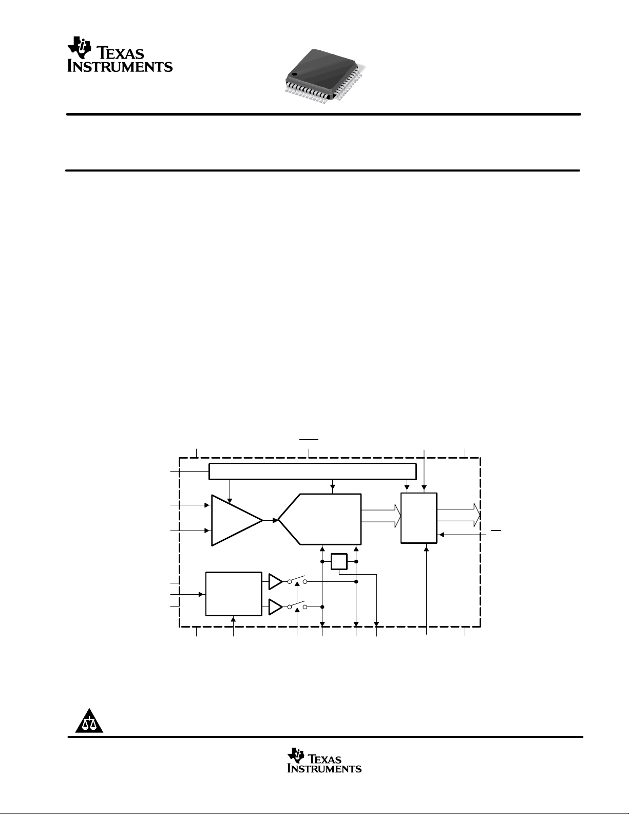
FUNCTIONAL BLOCK DIAGRAM
Timing Circuitry
CM
AGND BG PDREF REFT REFB CML DRGND DGND
CLK
AIN+
AIN–
NC
RBIAS
NC
AV
DD
STBY
DRV
DD
DV
DD
D[0–9]
OE
Sample
and Hold
10 Bit
ADC
3-State
Output
Buffers
Internal
Reference
Circuit
PRODUCTION DATA information is current as of publication date.
Products conform to specifications per the terms of Texas Instruments
standard warranty. Production processing does not necessarily include
testing of all parameters.
Copyright 2001, Texas Instruments Incorporated
Please be aware that an important notice concerning availability, standard warranty, and use in critical applications of
Texas Instruments semiconductor products and disclaimers thereto appears at the end of this data sheet.
Verzeichnis