
herunterladen
Product
Folder
Sample &
Buy
Technical
Documents
Tools &
Software
Support &
Community
AM1806
SPRS658F –FEBRUARY 2010–REVISED MARCH 2014
AM1806 ARM
®
Microprocessor
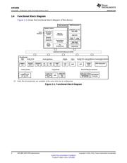
1 AM1806 ARM Microprocessor
1.1 Features
1
Output of the PRU Cores.
• 375- and 456-MHz ARM926EJ-S™ RISC MPU
– Standard Power-Management Mechanism
• Enhanced Direct Memory Access Controller 3
(EDMA3):
• Clock Gating
– 2 Channel Controllers
• Entire Subsystem Under a Single PSC Clock
Gating Domain
– 3 Transfer Controllers
– Dedicated Interrupt Controller
– 64 Independent DMA Channels
– Dedicated Switched Central Resource
– 16 Quick DMA Channels
• USB 2.0 OTG Port with Integrated PHY (USB0)
– Programmable Transfer Burst Size
– USB 2.0 High- and Full-Speed Client
• 1.8-V or 3.3-V LVCMOS I/Os (Except for USB and
DDR2 Interfaces)
– USB 2.0 High-, Full-, and Low-Speed Host
• Two External Memory Interfaces:
– End Point 0 (Control)
– EMIFA
– End Points 1,2,3,4 (Control, Bulk, Interrupt or
ISOC) RX and TX
• NOR (8- or 16-Bit-Wide Data)
• One Multichannel Audio Serial Port (McASP):
• NAND (8- or 16-Bit-Wide Data)
– Transmit and Receive Clocks
• 16-Bit SDRAM with 128-MB Address Space
– Two Clock Zones and 16 Serial Data Pins
– DDR2/Mobile DDR Memory Controller with one
– Supports TDM, I2S, and Similar Formats
of the following:
– DIT-Capable
• 16-Bit DDR2 SDRAM with 256-MB Address
Space
– FIFO Buffers for Transmit and Receive
• 16-Bit mDDR SDRAM with 256-MB Address
• Two Multichannel Buffered Serial Ports (McBSPs):
Space
– Transmit and Receive Clocks
• Three Configurable 16550-Type UART Modules:
– Supports TDM, I2S, and Similar Formats
– With Modem Control Signals
– AC97 Audio Codec Interface
– 16-Byte FIFO
– Telecom Interfaces (ST-Bus, H100)
– 16x or 13x Oversampling Option
– 128-Channel TDM
• LCD Controller
– FIFO Buffers for Transmit and Receive
• Two Serial Peripheral Interfaces (SPIs) Each with
• Video Port Interface (VPIF):
Multiple Chip Selects
– Two 8-Bit SD (BT.656), Single 16-Bit or Single
• Two Multimedia Card (MMC)/Secure Digital (SD)
Raw (8-, 10-, and 12-Bit) Video Capture
Card Interfaces with Secure Data I/O (SDIO)
Channels
Interfaces
– Two 8-Bit SD (BT.656), Single 16-Bit Video
• Two Master and Slave Inter-Integrated Circuits
Display Channels
( I
2
C Bus™)
• Universal Parallel Port (uPP):
• One Host-Port Interface (HPI) with 16-Bit-Wide
– High-Speed Parallel Interface to FPGAs and
Muxed Address and Data Bus For High Bandwidth
Data Converters
• Programmable Real-Time Unit Subsystem
– Data Width on Both Channels is 8- to 16-Bit
(PRUSS)
Inclusive
– Two Independent Programmable Real-Time Unit
– Single-Data Rate or Dual-Data Rate Transfers
(PRU) Cores
– Supports Multiple Interfaces with START,
• 32-Bit Load-Store RISC Architecture
ENABLE, and WAIT Controls
• 4KB of Instruction RAM per Core
• Real-Time Clock (RTC) with 32-kHz Oscillator and
• 512 Bytes of Data RAM per Core
Separate Power Rail
• PRUSS can be Disabled via Software to
• Three 64-Bit General-Purpose Timers (Each
Save Power
Configurable as Two 32-Bit Timers)
• Register 30 of Each PRU is Exported from
• One 64-Bit General-Purpose or Watchdog Timer
the Subsystem in Addition to the Normal R31
(Configurable as Two 32-Bit General-Purpose
1
An IMPORTANT NOTICE at the end of this data sheet addresses availability, warranty, changes, use in safety-critical applications,
intellectual property matters and other important disclaimers. PRODUCTION DATA.
Verzeichnis
- ・ Konfiguration des Pinbelegungsdiagramms on Seite 14 Seite 54
- ・ Abmessungen des Paketumrisses on Seite 240 Seite 241
- ・ Markierungsinformationen on Seite 240 Seite 241
- ・ Blockdiagramm on Seite 4 Seite 105 Seite 106 Seite 107 Seite 123
- ・ Technische Daten on Seite 59 Seite 60 Seite 61 Seite 62 Seite 63
- ・ Anwendungsbereich on Seite 2 Seite 245
- ・ Elektrische Spezifikation on Seite 63 Seite 64 Seite 65 Seite 66 Seite 67