
herunterladen
AP7115
Document number: DS31333 Rev. 11 - 2
1 of 12
www.diodes.com
January 2017
© Diodes Incorporated
AP7115
150mA LOW DROPOUT LINEAR REGULATOR WITH SHUTDOWN
Description
The AP7115 is a 150mA, fixed output voltage, low dropout linear
regulator. The device includes pass element, error amplifier, band
gap reference, current-limit and thermal shutdown circuit. The
characteristics of low dropout voltage and low quiescent current make
it suitable for use in battery powered devices. The typical quiescent
current is approximately 50µA. Several fixed output voltages are
available from 1.0V to 3.5V. Additional protection is provided with
built-in current-limit and thermal-shutdown functions.
Features
Wide Input Voltage Range from 2.5V to 5.5V
200mV Low Dropout Voltage at 150mA Output Current
Guaranteed 150mA Output Current
Low Quiescent Current 50µA
Output Voltage from 1.0V to 3.5V
±2% Output Voltage Accuracy
Low Temperature Drift at Output Voltage
High PSRR
Fast Transient Response
Current Limit Protection
Short Circuit Protection
Thermal Shutdown Protection
SOT25 and SOT353: Available in “Green” Molding Compound
(No Br, Sb)
Totally Lead-Free & Fully RoHS Compliant (Notes 1 & 2)
Halogen and Antimony Free. “Green” Device (Note 3)
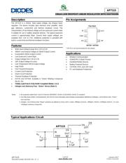
Pin Assignments
SOT25* / SOT353
IN
EN
BP
OUT
(Top View)
5
43
2
1
GND
* SOT25 is not recommended for new design.
Applications
Wireless Communication
GSM/GPRS Cellular Phones
Handheld Mobile Devices
Battery Powered Devices
CD-ROM, DVD, and LAN Cards
PC and Notebook Peripherals
Notes: 1. No purposely added lead. Fully EU Directive 2002/95/EC (RoHS) & 2011/65/EU (RoHS 2) compliant.
2. See http://www.diodes.com/quality/lead_free.html for more information about Diodes Incorporated’s definitions of Halogen- and Antimony-free, "Green"
and Lead-free.
3. Halogen- and Antimony-free "Green” products are defined as those which contain <900ppm bromine, <900ppm chlorine (<1500ppm total Br + Cl) and
<1000ppm antimony compounds.
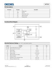
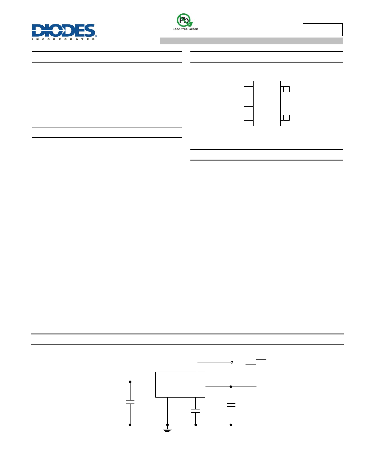
Typical Applications Circuit
IN
OUT
GND
AP7115
BP
EN
EN
V
IN
C
IN
C
BP
C
OUT
V
OUT
ON
OFF
1µF
0.1µF
1µF
Verzeichnis
- ・ Konfiguration des Pinbelegungsdiagramms on Seite 1 Seite 2
- ・ Abmessungen des Paketumrisses on Seite 10
- ・ Paket-Footprint-Pad-Layout on Seite 9 Seite 11
- ・ Teilenummerierungssystem on Seite 9
- ・ Markierungsinformationen on Seite 9
- ・ Blockdiagramm on Seite 2
- ・ Typisches Anwendungsschaltbild on Seite 1
- ・ Technische Daten on Seite 2
- ・ Anwendungsbereich on Seite 1
- ・ Elektrische Spezifikation on Seite 3