


herunterladen
1
®
AN1268.0
CAUTION: These devices are sensitive to electrostatic discharge; follow proper IC Handling Procedures.
1-888-INTERSIL or 1-888-468-3774
| Intersil (and design) is a registered trademark of Intersil Americas Inc.
Copyright © Intersil Americas Inc. 2010. All Rights Reserved
All other trademarks mentioned are the property of their respective owners.
ISL6327EVAL5: Voltage Regulator Coupled
Inductor Solution using the ISL6327 and ISL6609
Introduction
Today’s microprocessors are continuing towards higher
power consumption and functionality. Vcore regulators have
the burden of increasing load demands coupled with tighter
voltage regulation requirements. Power designers are
challenged with the design of high performance regulators
that can meet tight load regulation windows with increasing
maximum load and transient requirements and falling output
voltages. Add to that the push for higher efficiency solutions
and decreasing PCB real estate; meeting today’s
microprocessor power requirements is no simple task.
Intersil ISL6327 With Coupled Inductors
To help meet these design challenges Intersil offers a
complete reference design and evaluation package that
takes advantage of the features of the ISL6327 controller
and an output filter topology using coupled inductors and
fewer output capacitors.
The ISL6327 controls a microprocessor core voltage,
balances channel currents, and provides protective features
for up to 6 synchronous buck channels in parallel. The
controller uses a 8-bit DAC giving the user a digital interface
to select the output voltage, which is precisely regulated to
±0.5% accuracy using differential remote voltage sensing.
The DAC can be set up to read VR10 or VR11 VID codes.
Other features of the controller include overcurrent,
overvoltage, and undervoltage protection, internal over
temperature protection, programmable output voltage offset,
dynamic VID circuitry, and an IOUT pin that provides a
voltage proportional to the load current.
To meet the extremely fast load transients of
microprocessors the ISL6327 utilizes Intersil’s proprietary
Active Pulse Positioning (APA
TM
) and Adaptive Phase
Alignment (APA
TM
) modulation scheme and continuous
current sensing to achieve extremely fast load transient
response with fewer output capacitors.
‘Coupled’ with the fast control scheme a new approach to
the output filter can be implement using coupled inductors.
Coupling of two phases on one core allows the use of a
small output inductance for fast transient response without
taking the hit in efficiency due to higher individual phase
peak-to-peak current for an equivalent standard inductance.
The ISL6327 and ISL6609 datasheets along with the latest
documentation can be found on our website:
www.intersil.com.
ISL6327EVAL5 VRD Reference Design
The evaluation kit consists of the ISL6327EVAL5 evaluation
board, the ISL6327 datasheet, and this application note. The
evaluation board is designed to meet the output voltage and
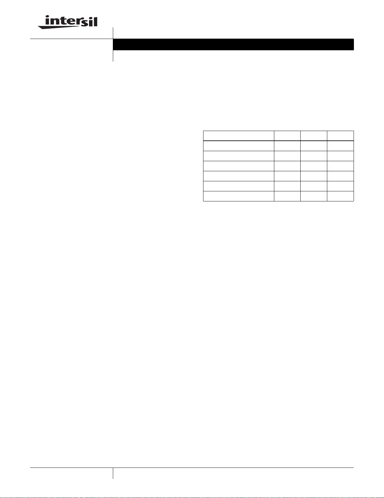
current specifications shown in Table 1, with the VID DIP
switches, SW2, set to 00101010 (1.35V).
The board is configured for down conversion from 12V to the
DAC setting. The evaluation board provides many test
points, two types of power supply connectors, an on-board
LGA775/771 socket for transient response evaluation and
terminal connectors for DC load testing. An on-board LED is
present to indicate the status of the PGOOD signal.
The printed circuit board is implemented in 6-layer, 1-ounce
copper. The layout and stackup are designed to emulate a
real world CPU/VCORE implementation. The board
schematic and BOM is provided at the end of the application
note.
Quick Start Evaluation
The ISL6327EVAL5 is designed for quick start-up and
evaluation. All that is required is a single ATX power supply.
To begin evaluating the ISL6327EVAL5 follow the steps
below.
1. Before doing anything to the evaluation board, make sure
the “Enable” switch (EN1) is in the OFF position.
2. Using an ATX power supply, connect the 24-pin main
power supply header to the “5V Power” connector
(5V_PWR1) on the board. Next connect the 4-pin 12V
header to the “12V Power” connector (12V_PWR1) on
the board.
3. Set the “Static VID” DIP switch (SW2) to 00101010
(VID7:0 as printed on the silkscreen).Set SW1 to 0001.
4. Move the “Enable” switch (S1) to the ON position to begin
regulation.
After step 4, the ISL6327EVAL5 should be regulating the
output voltage. The test points “TPVCORE1” and “TPGND1”
can be used to monitor the output voltage initially to verify
regulation.
TABLE 1. ISL6327EVAL5 DESIGN PARAMETERS
PARAMETER MAX TYPICAL MIN
No Load VCORE Regulation 1.35V 1.33V 1.31V
VCORE Tolerance +20mV -20mV
Load Line Slope 1.25mΩ
Continuous Load Current 130A
Load Current Step 100A
Load Current Transient 1200A/μs
Application Note October 26, 2010
Author: Jason Houston