


herunterladen
© Semiconductor Components Industries, LLC, 2009
May, 2009 − Rev. 0
1 Publication Order Number:
AND8276/D
AND8276/D
Theory of Operation of
V2 Controllers
with Emphasis on Applications using
MLCC’s for Output Filtering
Prepared by: Dennis Solley
ON Semiconductor
Every pulse width modulated controller configures basic
control elements such that when connected to the feedback
signal of a power converter, sufficient loop gain and
bandwidth is available to regulate the voltage set point
against line and load variations. These control elements
include error amplifier, pulse width modulator, ramp,
voltage reference, clock, latch and drive for the power
switch, which may or may not be integrated within the
controller. The arrangement of these elements differentiates
a voltage mode, or a current mode controller from a V2
device.
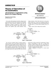
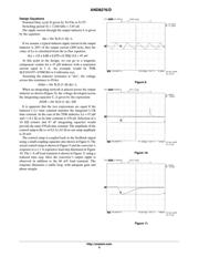
Figure 1 shows a basic voltage mode controller.
Figure 1. V Mode Control
Latch/Drive
Switch
Clock
PWM
Voltage Ramp
Error Amplifier
V
REF
V
FB
−
+
Z2
Z1
The converter’s feedback signal is compared against a
voltage reference and an error signal is generated at the
output of the voltage amplifier. This error signal is fed to one
input of a PWM, the other input being a voltage ramp of
fixed amplitude, generated from an internal clock. The
internal clock sets the latch to initiate a drive cycle. When the
error signal intersects the ramp, the PWM resets the latch
and the power switch is turned off. A small change in output
voltage, corresponding to input line or output load
variations, results in a change in the error voltage relative to
the ramp. This in turn causes the modulator’s duty cycle D
to change to regulate the output voltage.
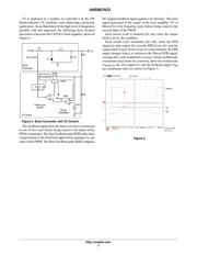
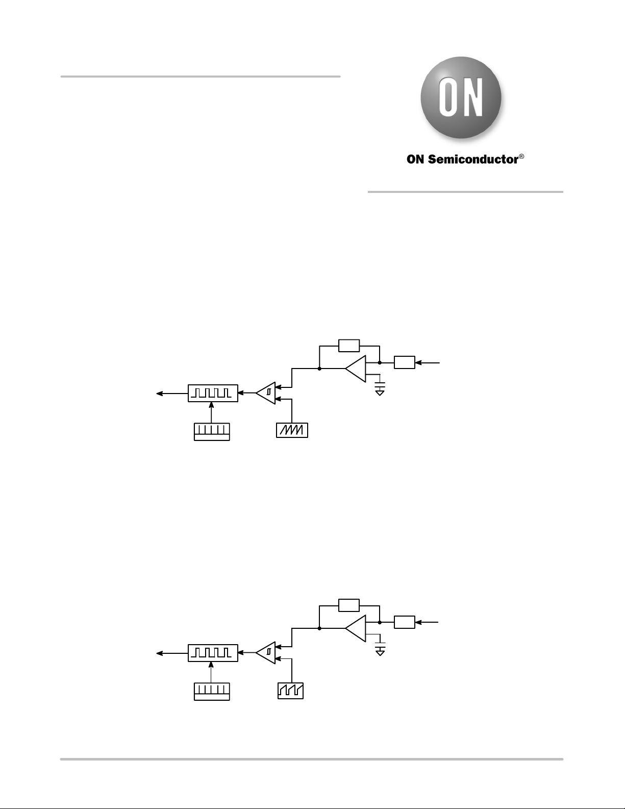
Figure 2 highlights the elements of a current mode
controller.
Figure 2. I Mode Control
Latch/Drive
Switch
Clock
PWM
Current Ramp
Error Amplifier
V
REF
V
FB
Z2
−
+
Z1
APPLICATION NOTE
http://onsemi.com
Verzeichnis