
herunterladen

User's Guide
SLUU412–March 2010
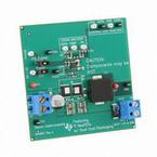
CSD163CEVM-591
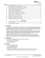
The CSD163CEVM-591 evaluation module (EVM) is a synchronous buck converter providing a fixed 1.2V
output at up to 25A from a 12-V input bus. The EVM is designed to start-up from a single supply; so, no
additional bias voltage is required for start-up. The module uses the TPS40304 high performance,
mid-input voltage synchronous buck controller and TI’s DualCool™ NexFET™ high performance
MOSFETs
TI’s DualCool™ NexFET™ family of power MOSFETs delivers an industry standard footprint, while
enabling thermally efficient cooling through the top and bottom of the package. This package allows power
system designers to effectively direct heat away from the PCB in high-current DC/DC applications,
resulting in improved power density, higher current capability and improved system reliability.
Contents
1 Description ................................................................................................................... 2
1.1 Applications ......................................................................................................... 2
1.2 Features ............................................................................................................. 2
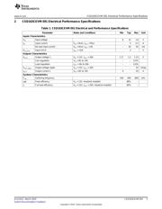
2 CSD163CEVM-591 Electrical Performance Specifications ............................................................ 3
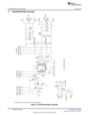
3 CSD163CEVM-591 Schematic ............................................................................................ 4
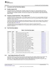
4 Connector and Test Point Descriptions .................................................................................. 5
4.1 Enable Jumper (JP2) .............................................................................................. 5
4.2 Frequency Spread Spectrum – FSS Jumper (JP1) ........................................................... 5
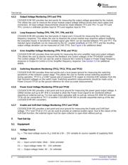
4.3 Test Point Descriptions ............................................................................................ 5
5 Test Set Up .................................................................................................................. 6
5.1 Equipment ........................................................................................................... 6
5.2 Equipment Setup ................................................................................................... 7
5.3 Heatsink Installation ............................................................................................... 9
5.4 Start Up/Shut Down Procedure .................................................................................. 9
5.5 Output Ripple Voltage Measurement Procedure ............................................................. 10
5.6 Control Loop Gain and Phase Measurement Procedure .................................................... 10
5.7 Equipment Shutdown ............................................................................................ 10
6 CSD163CEVM-591 Test Data ........................................................................................... 10
6.1 Efficiency .......................................................................................................... 11
6.2 Thermal Image (Emissivity Balanced See Section 5.1.6) ................................................... 11
6.3 Line and Load Regulation ....................................................................................... 12
6.4 Output Voltage Ripple ........................................................................................... 13
6.5 Switch Node ....................................................................................................... 13
6.6 Control Loop Bode Diagram .................................................................................... 14
6.7 Additional Waveforms ............................................................................................ 14
7 CSD163CEVM-591 Assembly Drawings and Layout ................................................................. 15
8 CSD163CEVM-591 Bill of Materials .................................................................................... 19
List of Figures
1 CSD163CEVM-591 Schematic............................................................................................ 4
2 CSD163CEVM-591 Recommended Test Set-Up....................................................................... 8
3 Output Ripple Measurement – Tip and Barrel using TP3 and TP4 .................................................. 8
4 Control Loop Measurement Setup........................................................................................ 9
DualCool, NexFET are trademarks of Texas Instruments.
Gap Pad is a registered trademark of .bergquist company.
1
SLUU412–March 2010 CSD163CEVM-591
Submit Documentation Feedback
Copyright © 2010, Texas Instruments Incorporated
Verzeichnis
- ・ Blockdiagramm on Seite 4
- ・ Technische Daten on Seite 3
- ・ Anwendungsbereich on Seite 21