


herunterladen

Maxim > Design Support > Technical Documents > Application Notes > General Engineering Topics > APP 3377
Maxim > Design Support > Technical Documents > Application Notes > Prototyping and PC-Board Layout > APP 3377
Keywords: Wafer Level Package, WLP, Flip Chip, Flip-Chip, CSP, Chip Scale Package, PCB Assembly,
PCBA, Die Product, Silicon Circuit, Silicon Die Circuit
APPLICATION NOTE 3377
Maxim Wafer-Level Package Assembly Guide
Nov 12, 2004
Abstract: Wafer-Level Packaging (WLP) allows an integrated circuit (IC) to be attached to a printed-circuit
board (PCB) face-down, with the chip's pads connecting to the PCB pads through individual solder balls. This
document describes the packaging technique and its advantages. It describes printed-circuit board (PCB)
layout and assembly process development for Maxim WLP.
Wafer-Level Packaging (WLP) uses individual solder balls to connect the integrated circuit (IC) to a printed-
circuit board (PCB). The IC is mounted face-down. This technology differs from other ball-grid array, leaded,
and laminate based CSPs because there are no bond wires or interposer connections. The principle
advantage is that IC-to-PCB board inductance is minimized. Secondary benefits are reduction in package size
and manufacturing cycle time, and enhanced thermal conduction characteristics.
This document describes printed-circuit board (PCB) layout and assembly process development for Maxim
WLP. Note that it is intended for initial PCB layout design and assembly process development and does not
assume any reliability objective for the customer end product. Customers still need to qualify their specified
end product life reliability requirements.
Package Construction
Maxim Package Outlines
The WLP solder bump interconnect is manufactured by building-up on a silicon wafer substrate. A film of BCB
(Benzocyclobutene) resin is applied over the wafer circuit surface. This film provides mechanical stress relief
for the ball attachment and electrical isolation at the die surface. Vias are imaged in the BCB film, providing
electrical contact to the IC bond pad. A UBM (Under Bump Metal) layer is added over vias. Typically, a
second application of BCB serves as a solder mask to define the diameter and position of reflowed solder
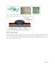
balls. Current package I/O designs include from two up to fifty-five solderable terminals, see Figure 1.
Standard solder bump alloys are eutectic Sn63Pb37, "High-Pb" Pb95Sn5, and "Pb-Free" Sn96.5Ag3Cu0.5. A
cross-section of a single WLP solder bump structure is shown in Figure 2. The backside of the component is
bare silicon with a laser inscribed Pin-1 designator and identification code. A double metal layer redistribution
(RDL) process allows for moving solder bumps from peripheral bond pads to any bump array pattern.
Page 1 of 11