
herunterladen

© 2006 Microchip Technology Inc. DS80242C-page 1
dsPIC30F6011A/
6012A/6013A/6014A
dsPIC30F6011A, dsPIC30F6012A,
dsPIC30F6013A, dsPIC30F6014A
(Rev. A2) Silicon Errata
The dsPIC30F6011A/6012A/6013A/6014A (Rev. A2)
samples you have received were found to conform to
the specifications and functionality described in the
following documents:
• DS70157 – “dsPIC30F/33F Programmer’s
Reference Manual”
• DS70143 – “dsPIC30F6011A, dsPIC30F6012A,
dsPIC30F6013A, dsPIC30F6014A Data Sheet”
• DS70046 – “dsPIC30F Family Reference Manual”
The exceptions to the specifications in the documents
listed above are described in this section. The specific
devices for which these exceptions are described are
listed below:
• dsPIC30F6011A
• dsPIC30F6012A
• dsPIC30F6013A
• dsPIC30F6014A
dsPIC30F601XA Rev. A2 silicon is identified by
performing a “Reset and Connect” operation to the
device using MPLAB
®
ICD 2 within the MPLAB IDE.
The following text is then visible under the MPLAB ICD 2
section in the output window within MPLAB IDE:
MPLAB ICD 2 Ready
Connecting to MPLAB ICD 2
...Connected
Setting Vdd source to target
Target Device dsPIC30F6014A found,
revision = Rev 0x1002
...Reading ICD Product ID
Running ICD Self Test
...Passed
MPLAB ICD 2 Ready".
The errata described in this section will be fixed in
future revisions of dsPIC30F6011A, dsPIC30F6012A,
dsPIC30F6013A and dsPIC30F6014A silicon.
Silicon Errata Summary
The following list summarizes the errata described in
further detail through the remainder of this document:
1. MAC Class Instruction with ±4 Address
Modification
Sequential MAC instructions, which prefetch data
from Y data space using ±4 address modification
will cause an address error trap.
2. Decimal Adjust Instruction
The Decimal Adjust instruction, DAW.b, may
improperly clear the Carry bit, C (SR<0>).
3. DISI Instruction
The DISI instruction will not disable interrupts if a
DISI instruction is executed in the same instruc-
tion cycle that the DISI counter decrements to
zero.
4. Output Compare Module in PWM Mode
Output compare will produce a glitch when loading
0% duty cycle in PWM mode. It will also miss the
next compare after the glitch.
5. Output Compare
The output compare module will produce a glitch
on the output when an I/O pin is initially set high
and the module is configured to drive the pin low at
a specified time.
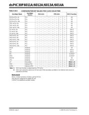
6. Using OSC2/RC15 as Digital I/O or CLKOUT
For this revision of silicon, pin OSC2/RC15 is oper-
ational for digital I/O and CLKOUT only in specific
oscillator modes.
7. LP Oscillator
For this revision of silicon, the LP Oscillator is not
operational.
8. INT0, ADC and Sleep Mode
ADC event triggers from the INT0 pin will not
wake-up the device from Sleep mode if the SMPI
bits are non-zero.
9. 4x and 8x PLL Mode
If 4x or 8x PLL mode is used, the input frequency
range is 5 MHz-10 MHz instead of 4 MHz-10 MHz.
The following sections will describe the errata and work
around to these errata, where they may apply.
dsPIC30F6011A/6012A/6013A/6014A Rev. A2 Silicon Errata