
herunterladen

AN-718
APPLICATION NOTE
One Technology Way • P.O. Box 9106 • Norwood, MA 02062-9106 • Tel: 781/329-4700 • Fax: 781/326-8703 • www.analog.com
TABLE OF CONTENTS
Evaluation Board Overview ............................................. 1
Evaluation Board Features ............................................... 1
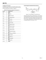
DIP Switch Link Options ................................................... 2
External Connectors ......................................................... 3
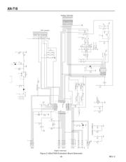
Demonstration Circuit ...................................................... 4
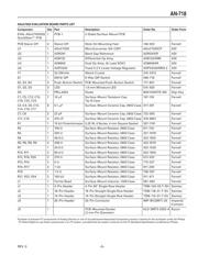
Parts List ............................................................................ 5
OVERVIEW
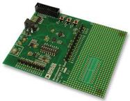
The ADuC7020 evaluation board has the following
features:
•
2-layer PCB (4” 5” form factor)
• 9 V power supply regulated to 3.3 V on board
• 4-pin UART header to connect to RS232 interface
cable
• 20-pin standard JTAG connector to connect to ULINK
emulator
• Demonstration circuit
• 32.768 kHz watch crystal to drive the PLL clock
• ADR291 2.5 V external reference chip
• Reset/Download/IRQ0 push-buttons
• Power indicator/general-purpose LEDs
• Access to all ADC inputs and DAC outputs from
external header. All device ports are brought out to
external header pins.
• Surface-mount and through-hole general-purpose
prototype area
Notes
1. This document refers to the MicroConverter ADuC7020
Evaluation Board Rev. A.
2. All references in this document to physical orientation
of components on the board are made with respect to a
component side view of the board, with the prototype
area appearing in the bottom of the board.
3. The board is laid out to minimize coupling between
the analog and digital sections of the board. The ground
plane is split with the analog section on the left-hand
side and a digital plane on the right-hand side of the
board. The regulated 3.3 V power supply is routed
directly to the digital section, and is ltered before being
routed into the analog section of the board.
ADuC7020 Evaluation Board Reference Guide
MicroConverter
®
ADuC7020 Development System
by Aude Richard
FEATURES
Power Supply
The user should connect the 9 V power supply via the
2.1 mm input power socket (J5). The input connector is
congured as CENTER NEGATIVE, i.e., GND on the cen-
ter pin and 9 V on the outer shield.
This 9 V supply is regulated via a linear voltage regula-
tor (U5). The 3.3 V regulator output is used to directly
drive the digital side of the board. The 3.3 V supply is
also ltered, and is then used to supply the analog side
of the board.
When on, the red LED (D3) indicates that a valid 3.3 V
supply is being driven from the regulator circuit. All
active components are decoupled with 0.1 F at device
supply pins to ground.
RS232 Interface
The ADuC7020 (U1) P1.1 and P1.0 lines are connected
to the RS232 interface cable via connector (J1). The
interface cable generates the required level shifting to
allow direct connection to a PC serial port. Ensure that
the cable supplied is connected to the board correctly,
i.e., DV
DD
is connected to DV
DD
, and DGND is connected
to DGND.
Emulation Interface
Nonintrusive emulation and download are possible on
the ADuC7020 via JTAG by connecting the ULINK emula-
tor to the J4 connector.
Crystal Circuit
The board is tted with a 32.768 kHz crystal from which
the on-chip PLL circuit can generate a 45 MHz clock.
External Reference (ADR291)
The external 2.5 V reference chip (U2) has two functions.
It is provided on the evaluation board to demonstrate the
external reference option of the ADuC7020, but its main
purpose is to generate the V
OCM
voltage of the differen-
tial amplier, if required.
Reset/Download/IRQ0 Push-Buttons
A RESET push-button is provided to allow the user to
manually reset the part. When inserted, the RESET pin of
the ADuC7020 is pulled to DGND. Because the RESET pin
on the ADuC7020 is Schmitt-triggered internally, there is
no need to use an external Schmitt trigger on this pin.
When inserted, the IRQ0 push-button switch drives
REV. 0
Verzeichnis