

herunterladen
1
®
AN1486.0
CAUTION: These devices are sensitive to electrostatic discharge; follow proper IC Handling Procedures.
1-888-INTERSIL or 1-888-468-3774
| Intersil (and design) is a registered trademark of Intersil Americas Inc.
Copyright Intersil Americas Inc. 2009. All Rights Reserved
All other trademarks mentioned are the property of their respective owners.
ISL6263AEVAL1Z, ISL6263BEVAL1Z
Evaluation Boards User Guide
Introduction
The ISL6263AEVAL1Z and ISL6263BEVAL1Z evaluation
boards demonstrate the performance of the ISL6263A and
ISL6263B respectively. The ISL6263A and ISL6263B are
single-phase synchronous buck PWM controllers, which
feature Intersil's Robust Ripple Regulator (R
3
) technology.
The evaluation board design criteria is located in Table 1. An
on-board dynamic-load generator is included for evaluating
the transient-load response. The dynamic-load applies a
2.5ms pulse of 200mΩ across V
OUT
and GND every 30ms.
What’s Inside
Contents of this document include:
• Recommended Test Equipment
• Interface Connections
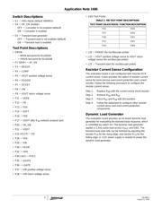
• Switch Descriptions
• Jumper Descriptions
• Test Point Descriptions
• Schematic
• Bill of Materials
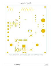
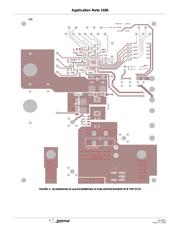
• Silkscreen Plots
• Board Layout Plots
Recommended Equipment
• (QTY 1) Adjustable 25V, 5A Power Supply
• (QTY 1) Fixed 12V, 100mA Power Supply
• (QTY 1) Fixed 5V, 100mA Power Supply
• (QTY 1) Adjustable 20A Constant Current Electronic Load
• (QTY 1) Digital Multi-Meter
• (QTY 1) Four-Channel Oscilloscope
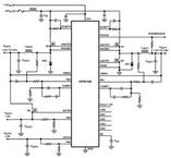
Interface Connections
• VIN: Input voltage to the power stage of the converter
- J6: VIN positive power input
- P37: VIN positive voltage sense
- J5: VIN return power input
- P38: VIN return voltage sense
• VOUT: Regulated output voltage from the converter
- J14: VOUT positive power output
- P5: VOUT positive voltage sense
- J13: VOUT return power output
- P9: VOUT return voltage sense
• 5V: +5V input voltage for VCC, PVCC, PGOOD-LED and
pull-up voltage rail
- J1: 5V positive input
- J2: 5V return input
• 3.3V: +3.3V input voltage for auxiliary circuits
- J3: 3.3V positive input
- J4: 3.3V return input
• +12V: +12V input voltage for the dynamic-load generator
- J11: 12V positive input
- J12: 12V return input
Jumper Descriptions
•J7 (SRIP) − Selects the logic state of the AF_EN pin
- Install shunt jumper across pins 1 and 2 for HIGH
- Install shunt jumper across pins 2 and 3 for LOW
(default)
•J9
− PGOOD circuit 5V input
- Shunt jumper installed during normal operation (default)
- Shunt jumper can be removed during efficiency tests
•J10 − Selects the logic state of the FDE pin
- Install shunt jumper across pins 1 and 2 for HIGH
- Install shunt jumper across pins 2 and 3 for LOW
(default)
•J16
− VDD input current measurement port
- Shunt jumper installed during normal operation (default)
- Shunt jumper replaced by DMM to measure VDD bias
current
•J17
− VDD and PVCC input current measurement port
- Shunt jumper installed during normal operation (default)
- Shunt jumper replaced by DMM to measure VDD bias
current and PVCC bias current
•J18
− PGOOD and pull-up supply selection
- Install shunt jumper across pins 1 and 2 for 5V (default)
- Install shunt jumper across pins 2 and 3 for 3.3V (3.3V
power supply should be connected to J3 and J4)
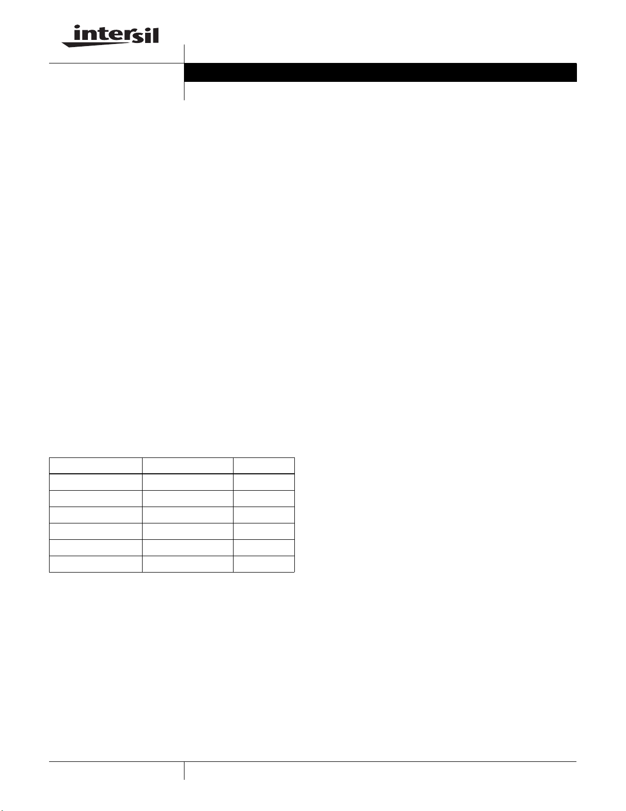
TABLE 1. EVALUATION BOARD DESIGN CRITERIA
PARAMETER VALUE UNITS
VIN 5 to 25 V
DC
VOUT 0.41200 to 1.28750 V
DC
DROOP 8 mΩ
FULL-LOAD 12 A
DC
PWM FREQUENCY 300 kHz
OCP ~15.5 A
DC
Application Note August 11, 2009
Verzeichnis