


herunterladen
Product
Folder
Sample &
Buy
Technical
Documents
Tools &
Software
Support &
Community
Reference
Design
MSP430F5438A
,
MSP430F5437A
,
MSP430F5436A
,
MSP430F5435A
MSP430F5419A, MSP430F5418A
SLAS655E –JANUARY 2010–REVISED JULY 2015
MSP430F543xA, MSP430F541xA Mixed-Signal Microcontrollers
1 Device Overview
1.1 Features
1
– Low-Frequency Trimmed Internal Reference
• Low Supply Voltage Range:
Source (REFO)
3.6 V Down to 1.8 V
– 32-kHz Crystals
• Ultra-Low Power Consumption
– High-Frequency Crystals up to 32 MHz
– Active Mode (AM):
All System Clocks Active • 16-Bit Timer TA0, Timer_A With Five
230 µA/MHz at 8 MHz, 3.0 V, Flash Program Capture/Compare Registers
Execution (Typical)
• 16-Bit Timer TA1, Timer_A With Three
110 µA/MHz at 8 MHz, 3.0 V, RAM Program
Capture/Compare Registers
Execution (Typical)
• 16-Bit Timer TB0, Timer_B With Seven
– Standby Mode (LPM3):
Capture/Compare Shadow Registers
Real-Time Clock (RTC) With Crystal, Watchdog,
• Up to Four Universal Serial Communication
and Supply Supervisor Operational, Full RAM
Interfaces
Retention, Fast Wakeup:
– USCI_A0, USCI_A1, USCI_A2, and USCI_A3
1.7 µA at 2.2 V, 2.1 µA at 3.0 V (Typical)
Each Support:
Low-Power Oscillator (VLO), General-Purpose
• Enhanced UART Supports Automatic Baud-
Counter, Watchdog, and Supply Supervisor
Rate Detection
Operational, Full RAM Retention, Fast Wakeup:
• IrDA Encoder and Decoder
1.2 µA at 3.0 V (Typical)
• Synchronous SPI
– Off Mode (LPM4):
– USCI_B0, USCI_B1, USCI_B2, and USCI_B3
Full RAM Retention, Supply Supervisor
Each Support:
Operational, Fast Wakeup:
1.2 µA at 3.0 V (Typical)
• I
2
C
– Shutdown Mode (LPM4.5):
• Synchronous SPI
0.1 µA at 3.0 V (Typical)
• 12-Bit Analog-to-Digital Converter (ADC)
• Wake up From Standby Mode in 3.5 µs (Typical)
– Internal Reference
• 16-Bit RISC Architecture
– Sample-and-Hold
– Extended Memory
– Autoscan Feature
– Up to 25-MHz System Clock
– 14 External Channels, 2 Internal Channels
• Flexible Power-Management System
• Hardware Multiplier Supports 32-Bit Operations
– Fully Integrated LDO With Programmable
• Serial Onboard Programming, No External
Regulated Core Supply Voltage
Programming Voltage Needed
– Supply Voltage Supervision, Monitoring, and
• Three-Channel Internal DMA
Brownout
• Basic Timer With RTC Feature
• Unified Clock System
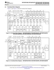
• Section 3 Summarizes the Available Family
– FLL Control Loop for Frequency Stabilization
Members
– Low-Power Low-Frequency Internal Clock
• For Complete Module Descriptions, See the
Source (VLO)
MSP430x5xx and MSP430x6xx Family User's
Guide (SLAU208)
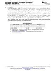
1.2 Applications
• Analog and Digital Sensor Systems • Thermostats
• Digital Motor Controls • Digital Timers
• Remote Controls • Hand-Held Meters
1
An IMPORTANT NOTICE at the end of this data sheet addresses availability, warranty, changes, use in safety-critical applications,
intellectual property matters and other important disclaimers. PRODUCTION DATA.
Verzeichnis
- ・ Konfiguration des Pinbelegungsdiagramms on Seite 7 Seite 8 Seite 9 Seite 69 Seite 71
- ・ Abmessungen des Paketumrisses on Seite 6 Seite 100 Seite 101 Seite 103 Seite 104
- ・ Markierungsinformationen on Seite 97 Seite 100 Seite 101
- ・ Blockdiagramm on Seite 3 Seite 68
- ・ Typisches Anwendungsschaltbild on Seite 2
- ・ Technische Daten on Seite 15 Seite 16 Seite 17 Seite 18 Seite 19
- ・ Anwendungsbereich on Seite 1 Seite 88 Seite 102 Seite 108