

herunterladen

1
Application Note 1856
ISL28617VYADJEV1Z User’s Guide
Introduction
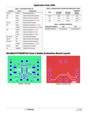
The ISL28617VYADJEV1Z User’s Guide evaluation board is
designed to assess the ISL28617 instrumentation amplifier’s
(in-amp) performance with Bulk Metal® Foil resistors from
Vishay Precision Group. With a differential input voltage range up
to ±34V, a supply voltage range of 8V (±4V) to 40V (±20V) and gain
ranging from 0.1 to 10,000, this precision in-amp is ideal for a
wide variety of applications. It features differential inputs and
outputs, and can drive the output rail-to-rail. The gain accuracy is
limited only by the matching of the gain resistors. Reference:
Vishay Precision Group’s foil resistors at
http://www.vishaypg.com/ppg?63209
.
The FRSM series Bulk Metal® Foil ultra-high precision resistors
have a tolerance of 0.01% and a temperature coefficient (TCR) of
0.2 ppm/°C, giving exceptional gain accuracy that is ideal for
high end applications. The foil resistors are capable of achieving
tighter absolute and ratio tolerances than any other technology.
The real value of foil resistors is their unmatched stability
through temperature excursions, load life and extraordinary
thermal and environmental stresses, resulting in far more stable
gain ratios. Another important feature of the Bulk Metal® Foil
technology is the lowest current noise of any resistor technology
(≤ 40 dB). The combination of foil resistors’ low current noise and
the exceptional low-noise performance of the ISL28617 amplifier
make this the perfect solution for noise critical precision
applications.
The board is configured for ease of use, but allows for more
complex variations to fit the user’s need. The evaluation board
includes test points (V
CC
, V
EE
, and GND) for the power supply
inputs, and is configured for operation from split supplies
between ±4V to ±20V. There are two pairs of test points for the
differential input and output as well (V
IN+
, V
IN-
, V
OUT+
, and V
OUT-
).
The board requires the user to provide the gain resistors R1 and R2.
Table 1 gives suggested resistor values for gains of: 0.25, 10 and
100. Ordering information is shown in Table 3.
Reference Documents
• ISL28617 Data sheet, FN6562
• FRSM Vishay Foil Resistor Data sheet, Document Number:
63209
Power Supplies
External power connections are made to the positive supply rail
(TP1), the negative supply rail (TP9), and ground (TP4) for split
supply operation. The operating voltage range is ±4V to ±20V.
The in-amp has two distinct sets of power supplies; one on the
input stage and one on the output stage. For the evaluation
board, the output stage supplies are tied to the input stage
supplies, and the common mode voltage is tied to ground. The
supply voltage on the input stage must be 3V above and below
the maximum and minimum input signal voltage, respectively.
Note that while the output stage is rail-to-rail, the feedback
returns to the input stage, which is not rail-to-rail. Therefore, the
input power supply must be 3V above and below the maximum
and minimum output signal as well. Table 2 provides suggested
supply voltages for the three standard boards. For more
information, reference “Setting the Power Supply Voltages” on
page 13 of the ISL28617 data sheet.
If the user wants to control the output supplies separately, the R3
and R5 resistors must be removed, and the V
CO
(TP2) and V
EO
(TP6) test points are used for the positive output supply and
negative output supply respectively (reference evaluation board
schematic in Figure 4). Single supply operation requires
removing R7 and attaching the desired common mode voltage to
the V
REF
(TP10) test point. Using the separate supply feature
enables input signals riding on a high common mode voltage to be
level shifted to a low voltage device, such as an analog to digital
converter (ADC). The rail-to-rail output stage can be powered from
the same supplies as the ADC while preserving the in-amp’s
maximum input dynamic range. Once again, the positive input
power supply must be 3V above the maximum output signal, and
the negative input power supply must be 3V below the minimum
output signal.
Amplifier Configuration
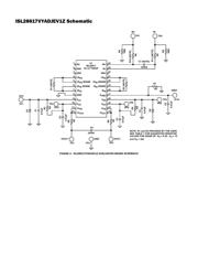
The ISL28617 evaluation board schematic is shown in Figure 4.
The User will first have to select the gain of the amplifier and
solder in resistors R1 and R2. The board is configured for split
supply operation with input and output supplies tied together.
Gain options for 0.25, 10 and 100, with the required resistor and
capacitor changes are listed in Table 1. The in-amp gain is
controlled through R1 and R2, the feedback and input resistors,
with the following simple formula:
R1 and R2 also limit the maximum signal size at the input and
output due to the amplifier architecture. Table 2 shows the signal
limits for the boards at the preset resistor values. For more
information, refer to “Setting the Feedback Gain R
FB
" and
“Setting the Input Gain R
IN
” on page 13 of the ISL28617 data
sheet.
The evaluation board allows the user to add an optional low pass
RC filter to the signal path. R8, R9, and C6 create a filter on the
output of the in-amp, while R10, R11, and C7 create a filter on
the input.
A
V
R1
R2
-------
=
(EQ. 1)
CAUTION: These devices are sensitive to electrostatic discharge; follow proper IC Handling Procedures.
1-888-INTERSIL or 1-888-468-3774
| Copyright Intersil Americas LLC 2013. All Rights Reserved
Intersil (and design) is a trademark owned by Intersil Corporation or one of its subsidiaries.
All other trademarks mentioned are the property of their respective owners.
June 24, 2013
AN1856.0
Verzeichnis