

herunterladen
1
®
AN1265.0
CAUTION: These devices are sensitive to electrostatic discharge; follow proper IC Handling Procedures.
1-888-INTERSIL or 1-888-468-3774
| Intersil (and design) is a registered trademark of Intersil Americas Inc.
Copyright Intersil Americas Inc. 2006. All Rights Reserved
All other trademarks mentioned are the property of their respective owners.
ISL6273EVAL1 Evaluation Board
Application Manual
Introduction
The ISL6273EVAL1 board provides a convenient platform to
evaluate the performance of the ISL6273 low-quiescent
high-efficiency step-down switching regulator. The ISL6273
is a 1.5MHz, 1.2A adjustable output voltage regulator. The
output voltage is set by a resistor divider consisting of R1
and R2 on the board. The output voltage is set to 1.6V in the
evaluation board but can be modified by changing the R2
value. The evaluation board also allows users to evaluate
the forced PWM or PFM operation mode at light load and the
behavior of the POR signal.
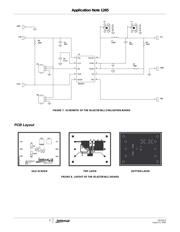
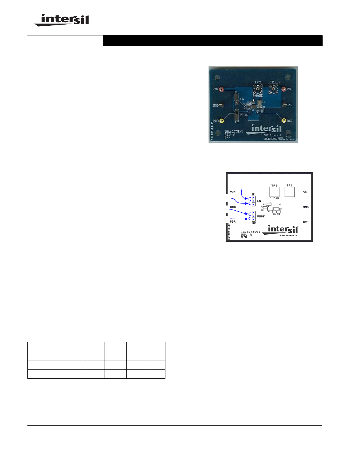
ISL6273EVAL1 Evaluation Board
A photo of the ISL6273EVAL1 board is shown in Figure 1.
The schematic, layout and bill-of-materials (BOM) are given
at the end of this application note. The complete regulator is
located at the center of the board. Various connectors and
jumpers are provided for the convenience of the evaluation.
On the left side of the board are the connectors for the input
power source (Red: VIN; Black: GND). The output
connectors are located on the right side (Red: VO; Black:
GND). The two yellow test points are for the RSI and POR
signals respectively, as labelled on the board. The RSI input
needs either be driven to a low or a high logic input. Do not
leave the RSI input signal floating. The open-drain POR
signal is pulled up to VIN through a 100kΩ resistor (R3), as
shown in the schematics. Jumper H1 allows the user to
enable or disable the IC. Jumper H2 is the mode selection
input. Do not leave the EN or the MODE signal floating.
The settings for the two jumpers are shown in Figure 2. The
evaluation board also offers two oscilloscope probe tip
connectors to minimize the switching noise on the
waveforms. TP1 is the connector for the output voltage and
TP2 is the PHASE signal.
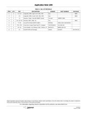
Specifications
Table 1 shows the electrical specification of the regulator in
the evaluation board.
Evaluation Board Setup
The following are steps for setting up the evaluation board:
1. Connect Jumper H1 at the position of Enable.
2. Connect Jumper H2 either at the position of PFM or
Forced PWM, but do not leave it floating.
3. Connect the RSI input to either ground or VIN. Do not
leave it floating.
4. Connect a power supply with an output voltage between
2.7V to 5.5V to VIN and GND connectors. Make sure the
power supply has enough current capability (1A
recommended).
5. Connect the output to a load (resistor or electronic load).
6. Turn on the input power supply.
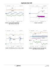
Typical Operating Characteristics
This section shows typical waveforms and performance
captured from the evaluation board.
TABLE 1. ELECTRICAL SPECIFICATIONS.
PARAMETER MIN TYP MAX UNIT
Input Voltage 2.7 - 5.5 V
Output Voltage (Note) - 1.6 - V
Output Current 1.2 - - A
NOTE: The output voltage can be set to other values by changing the
R2 value.
FIGURE 1. PHOTO OF THE ISL6273EVAL1 BOARD
FIGURE 2. SETTINGS FOR JUMPERS H1 AND H2
Enable
Disable
PFM
Forced PWM
Application Note August 22, 2006
Verzeichnis
- ・ Blockdiagramm on Seite 3
- ・ Technische Daten on Seite 1
- ・ Elektrische Spezifikation on Seite 1