


herunterladen
1
ISL8120EVAL4Z Evaluation Board Setup Procedure
Description
The ISL8120 integrates two voltage-mode synchronous buck
PWM controllers. It can be used either for dual independent
outputs or a 2-phase single-output regulator.
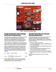
The ISL8120EVAL4Z evaluation board is used for performance
demo of 2/n-phase single-output applications. This application
note introduces the setup procedure and performance of the
ISL8120EVAL4Z evaluation board.
The ISL8120EVAL3Z evaluation board is for performance
demo of dual independent outputs and DDR applications.
Refer to application note AN1528
“ISL8120EVAL3Z Evaluation
Board Setup Procedure” for details of the ISL8120EVAL3Z
board.
References
• ISL8120 datasheet
Recommended Equipment
• 0V to 22V power supply with at least 20A source current
capability, battery, or notebook AC adapter.
• Two electronic loads capable of sinking current up to 30A.
• Digital multimeters (DMMs).
• 100MHz quad-trace oscilloscope.
Quick Start
1. Ensure that the circuit is correctly connected to the supply
and loads prior to applying any power.
2. Adjust the input supply to be 12V. Turn on the input power
supply.
3. Verify the output voltage is 1.2V. If PGOOD is set high, the
LED2 will be green. If PGOOD is set low, the LED2 will be
red. TP4 is the test post to monitor PGOOD.
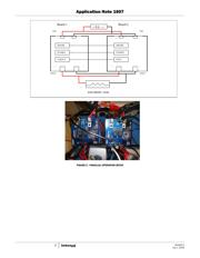
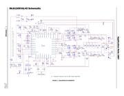
Circuits Description
J1 and J2 are the input power terminals.
J3 and J4 are output lugs for load connections.
The input electrolytic capacitors are used to handle the input
current ripples.
Two upper and two lower Renesas “speed” series LFPAK
MOSFETs are used for each phase.
320nH PULSE surface mount inductors are used for each
phase. Under the 500kHz setup, the inductor current
peak-to-peak ripple is 7.5A at 12V input and 1.2V output.
Four SANYO POSCAP 2R5TPF470M7L (7mΩ) are used as
output E-caps.
TP2 and TP3 are remote sense posts. These pins can be used
to monitor and evaluate the system voltage regulations. If the
user wants to use these test posts for remote sense, the R
29
and R
31
need to be changed to higher values, such as 10Ω.
Also, the related voltage sense divider needs to be increased to
a higher resistance, such as 1k.
TP1 is a test socket to hold the scope probe to check the
output waveforms.
JP9 is used to disable the part.
JP6 is for connection of inputs of clock signal for the part to be
synchronized with.
JP5 is used for connection of ISHARE signals of multiple
boards in parallel operation applications.
JP3, JP4, R
15
and R
17
are used to set up the phase shift
between the 2 phases of the IC.
R
27
is used to isolate the noise at PVCC caused by driving. In
3.3V applications, it is recommended to short R
27
to 0 in order
to prevent VCC from dropping below POR under low input
voltage.
Evaluating the Other Output
Voltage
The ISL8120EVAL4Z kit output is preset to 1.2V/50A. V
OUT1
can also be adjusted between 0.6V to 3V by changing the value
of R
26
and R
6
for V
OUT
, as given by Equation 1. The same rule
applies for V
OUT2
.
Ordering Information
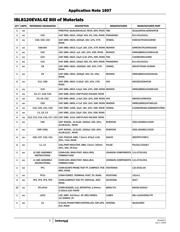
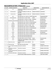
PART NUMBER DESCRIPTION
ISL8120EVAL4Z IISL8120EVAL4Z evaluation board
R
26
R
6
V
OUT
V
REF
1–
-------------------------------------------------
=
where V
REF
= 0.6V
(EQ. 1)
July 1, 2016
AN1607.2
Application Note 1607
CAUTION: These devices are sensitive to electrostatic discharge; follow proper IC Handling Procedures.
1-888-INTERSIL or 1-888-468-3774
| Copyright Intersil Americas LLC 2010, 2013, 2016. All Rights Reserved
Intersil (and design) is a trademark owned by Intersil Corporation or one of its subsidiaries.
All other trademarks mentioned are the property of their respective owners.
Verzeichnis