
herunterladen
1
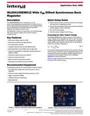
Application Note 1860
ISL85415DEMO1Z Wide V
IN
500mA Synchronous Buck
Regulator
Description
The ISL85415DEMO1Z kit is intended for use for
point-of-load applications sourcing from 3V to 36V. The kit is
used to demonstrate the performance of the ISL85415 Wide
V
IN
Low Quiescent Current High Efficiency Sync Buck
Regulator with 500mA output current.
The ISL85415 is offered in a 4mmx3mm 12 Ld DFN package
with 1mm maximum height. The converter occupies
1.516 cm
2
area.
Key Features
• Wide input voltage range 3V to 36V
• Synchronous operation for high efficiency
• No compensation required
• Integrated high-side and low-side NMOS devices
• Selectable PFM or forced PWM mode at light loads
• Internal fixed (500kHz) or adjustable switching frequency
300kHz to 2MHz
• Continuous output current up to 500mA
•Internal or external soft-start
• Minimal external components required
• Power-good and enable functions available
Recommended Equipment
The following materials are recommended to perform testing:
• 0V to 50V power supply with at least 2A source current
capability
• Electronic Loads capable of sinking current up to 1.5A
• Digital multimeters (DMMs)
• 100MHz quad-trace oscilloscope
• Signal generator
Quick Setup Guide
1. Ensure that the circuit is correctly connected to the supply
and loads prior to applying any power.
2. Connect the bias supply to VIN, the plus terminal to VIN (P4)
and the negative return to GND (P5).
3. Turn on the power supply.
4. Verify the output voltage is 3.3V for V
OUT.
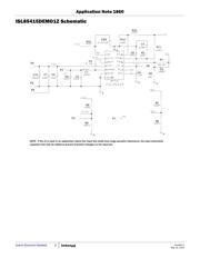
Evaluating the Other Output Voltage
The ISL85415DEMO1Z kit output is preset to 3.3V; however,
output voltages can be adjusted from 0.6V to 15V. The output
voltage programming resistor, R
2
, will depend on the desired
output voltage of the regulator and the value of the feedback
resistor R
1
, as shown in Equation 1.
If the output voltage desired is 0.6V, then R
1
is shorted. Please
note that if V
OUT
is less than 1.8V, the switching frequency and
compensation must be changed for 300kHz operation due to
minimum on-time limitation. Please refer to datasheet
ISL85415
for further information.
Table 1 on page 2 shows the component selection that should
be used for the respective V
OUTs
.
R
2
R
1
0.6
V
OUT
0.6–
---------------------------
=
(EQ. 1)
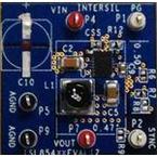
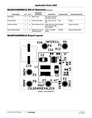
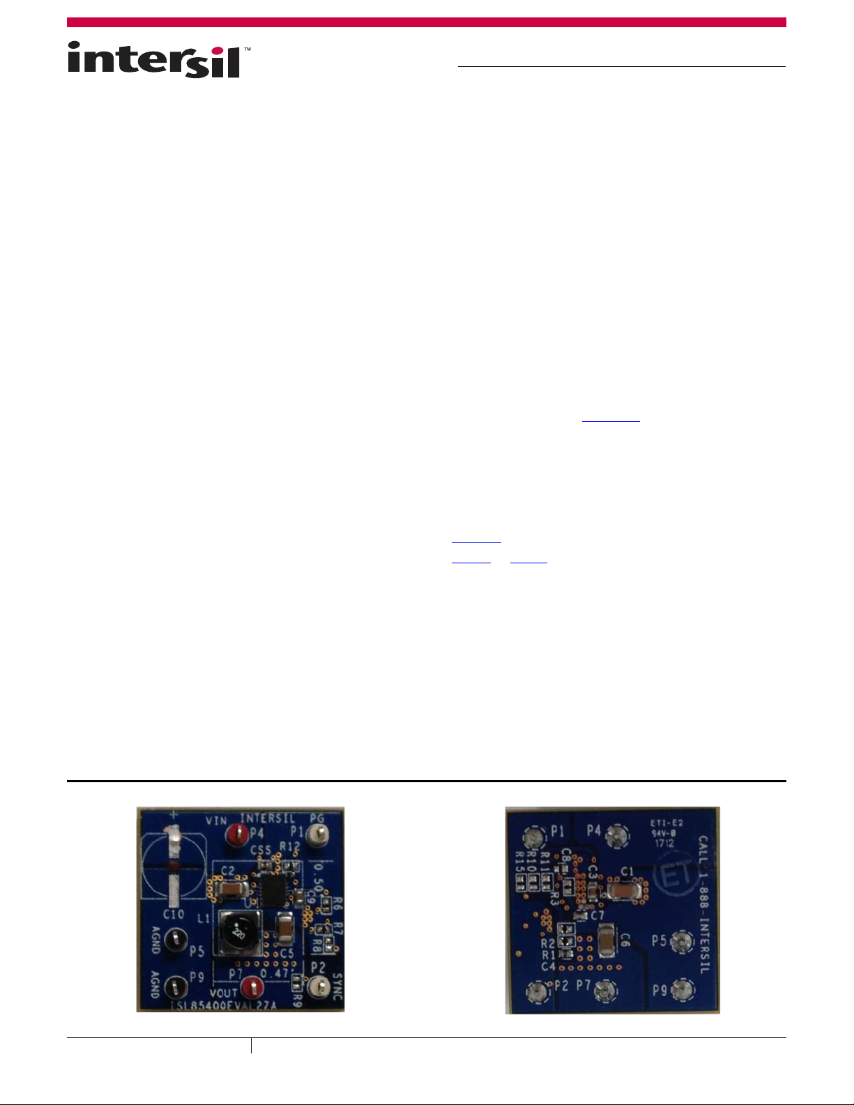
FIGURE 1. FRONT OF EVALUATION BOARD ISL85415DEMO1Z
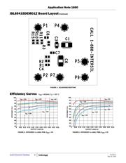
FIGURE 2. BACK OF EVALUATION BOARD ISL85415DEMO1Z
May 16, 2014
AN1860.2
CAUTION: These devices are sensitive to electrostatic discharge; follow proper IC Handling Procedures.
Copyright Intersil Americas LLC 2013, 2014. All Rights Reserved.
1-888-INTERSIL or 1-888-468-3774
| Intersil (and design) is a trademark owned by Intersil Corporation or one of its subsidiaries.
All other trademarks mentioned are the property of their respective owners.
Verzeichnis