
1
®
ISL88550AEVAL1Z Kit: Synchronous Step Down
Controller with Sourcing and Sinking LDO Regulator
General Description
ISL88550A integrates a synchronous buck PWM controller
to generate VDDQ, a sourcing and sinking LDO linear
regulator to generate VTT, and a 10mA reference output
buffer to generate VTTR. The buck controller drives two
external N-Channel MOSFETs to generate output voltages
down to 0.7V from a 2V to 25V input with output currents up
to 15A. The LDO can sink or source up to1.5A continuous
and 2.5A peak current with fast response. Both the LDO
output and the 10mA reference buffer output can be made to
track the REFIN voltage via a built-in resistive divider. These
features make the ISL88550A ideally suited for DDR
memory applications in desktops, notebooks and graphic
cards.
The PWM controller in the ISL88550A uses constant-on-time
PWM architecture with a programmable switching frequency
of up to 600kHz. This control scheme handles wide
input/output voltage ratios with ease and provides 100ns
“instant-on” response to load transients while maintaining
high efficiency and a relatively constant switching frequency.
The ISL88550A offers full programmable UVP/OVP and skip
mode options ideal in portable applications. Skip mode
allows for improved efficiency at lighter loads.
The VTT and VTTR outputs track to within 1% of VREFIN/2.
The high bandwidth of this LDO regulator allows excellent
transient response without the need for bulk capacitors, thus
reducing the cost and size.
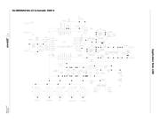
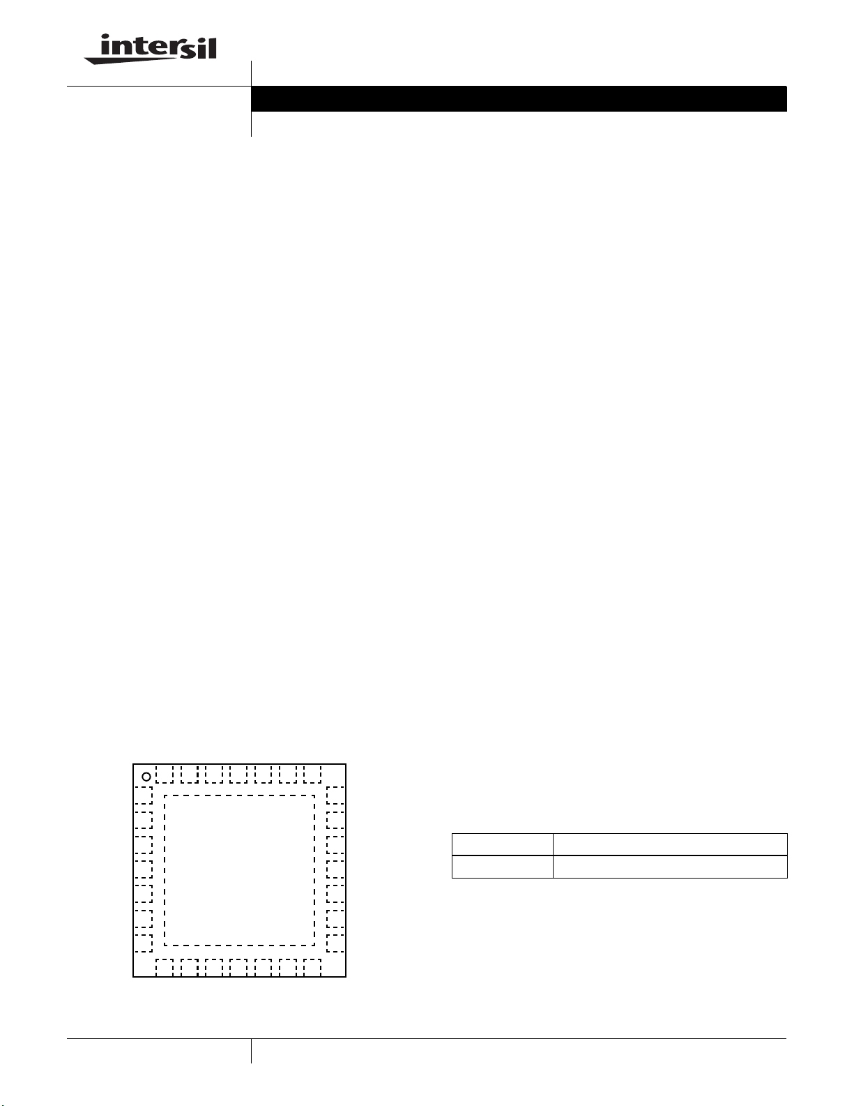
Pinout
ISL88550A
(28 LD TQFN)
TOP VIEW
Features
Buck Controller
• Constant-On PWM with 100ns Load-Step Response
• Up to 95% Efficiency
• 2V to 25V Input Voltage Range
• 1.8V/2.5V fixed or 0.7V to 3.5V Adjustable Output
• 200kHz, 300kHz, 450kHz, 600kHz Switching Frequencies
• Programmable Current Limit with Foldback Capability
• 1.7ms Digital Soft-Start and Independent Shutdown
• Overvoltage/Undervoltage Protection Option
• Power-Good Window Comparator
LDO Section
• Fully Integrated VTT and VTTR Capability
• VTT has ±2.5A Sourcing/Sinking Capability
• VTT and VTTR Outputs Track VREFIN/2
• VTT and VTTR within 1% of VREFIN/2
• All Ceramic Output Capacitor Designs
• 1.0V to 2.8V Input REFIN Range
• Analog Soft-Start Option and Independent Shutdown
• Power-Good Window Comparator
Applications
• DDR I and DDR II Memory Power Supplies
• Desktop Computers
• Notebooks and Desknotes
• Graphics Cards
• Game Consoles
• Networking and RAID
SS
VTTS
VTTR
PGND2
VTT
VTTI
REFIN
TPO
SHDNA#
AVDD
SKIP#
GND
PGND1
VDD
FB
OUT
VIN
UGATE
PHASE
BOOT
LGATE
1
2
3
4
5
6
7
21
20
19
18
17
16
15
28 27 26 25 24 23 22
8 9 10 11 12 13 14
STBY#
POK2
POK1
ILIM
REF
OVP/UVP
TON
Ordering Information
PART PACKAGE
ISL88550AEVAL1Z Evaluation Board
July 23, 2008 AN1200.3Application Note
CAUTION: These devices are sensitive to electrostatic discharge; follow proper IC Handling Procedures.
1-888-INTERSIL or 1-888-468-3774
| Intersil (and design) is a registered trademark of Intersil Americas Inc.
Copyright Intersil Americas Inc. 2006, 2008. All Rights Reserved
All other trademarks mentioned are the property of their respective owners.
Verzeichnis