
herunterladen
FB
PGOOD
VIN
LM21212-1
VOUT
AGND
COMP
PVIN
SYNC
SW
EN
C6
L1
R
C1
C
C1
C
C2
C
C3
R
FB1
R
FB2
R
C2
PGND
AVIN
C1
1
11-16
3
4
17
19
18
20
8,9,10
5,6,7
R1
SS /
TRK
C
SS
2
eTSSOP-20
C7
C8
Vin
R
PG
C3 C4 C5
SYNC
SS_TRK
R
AC
ENABLE
R
EN1
R
EN2
GND
GND
C9
PGOOD
SWITCH
AC INJ
VOUT
SENSE+
VOUT
SENSE-
VIN
SENSE-
VIN
SENSE+
V
IN
= 2.95V to 5.5V
V
OUT
= 1.2V, up to 12A
0.1 éF
820 pF
165Ö
10 kÖ
49.9Ö
10 kÖ
7.32 kÖ
2700 pF
82 pF
10 kÖ
100 éF
0.56 éH
100 éF
open
open
1Ö
1 éF
0.033 éF
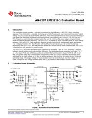
User's Guide
SNVA467B–February 2011–Revised May 2013
AN-2107 LM21212-1 Evaluation Board
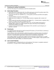
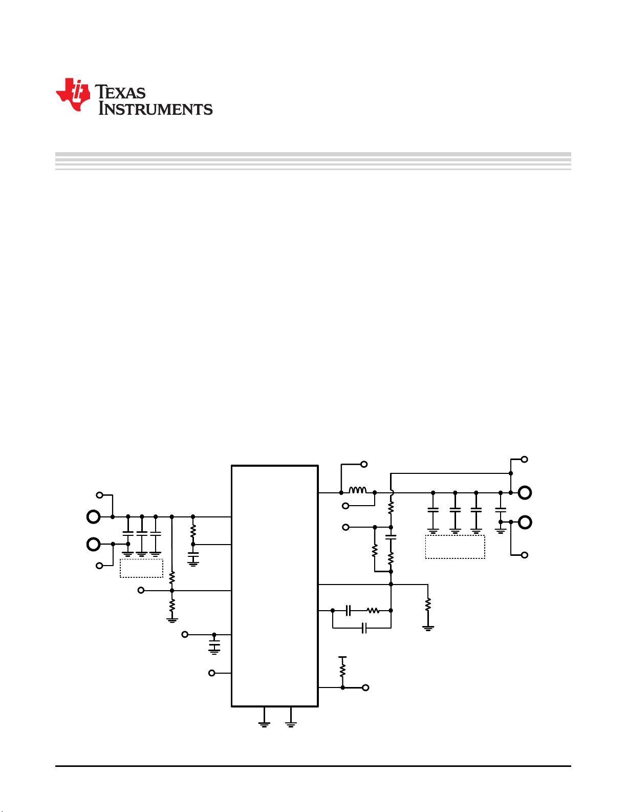
1 Introduction
This evaluation board provides a solution to examine the high efficiency LM21212-1 buck switching
regulator. The LM21212-1 is capable of driving up to 12A of continuous load current with excellent output
voltage accuracy due to its ±1% internal reference. This device also features a clock synchronization input
that allows the switching frequency to be synchronized to an external clock source. The 300 kHz to 1.5
MHz frequency synchronization range enables the user to minimize the power stage component size,
while still allowing for high efficiency. The LM21212-1 is capable of down converting from an input voltage
between 2.95V and 5.5V. Fault protection features include current limit, output power good, and output
over-voltage protection. The dual function soft-start/tracking pin can be used to control the startup
response of the LM21212-1, and the precision enable pin can be used to easily sequence the LM21212-1
in applications with sequencing requirements.
The LM21212-1 evaluation board has been optimized to work from 2.95V to 5.5V, achieving a balance
between overall solution size and regulator efficiency. The evaluation board measures just under 2” x 2”
on a four layer PCB, and exhibits a junction-to-ambient thermal impedance (θ
JA
) of 24°C/W with no air
flow. The power stage and compensation components of the LM21212-1 evaluation board have been
optimized for an input voltage of 5V, but for testing purposes, the input can be varied across the entire
operating range. The output voltage of the evaluation board is nominally 1.2V, but this voltage can be
easily changed to any voltage between 0.6V and V
IN
by modifying the feedback resistor network.
2 Evaluation Board Schematic
Figure 1. Evaluation Board Schematic
All trademarks are the property of their respective owners.
1
SNVA467B–February 2011–Revised May 2013 AN-2107 LM21212-1 Evaluation Board
Submit Documentation Feedback
Copyright © 2011–2013, Texas Instruments Incorporated
Verzeichnis