
herunterladen

t
ON
=
1.18 x 10
-10
x (R1
+ 1.4k)
(V
IN
- 1.4V)
+ 67 ns
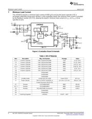
J1
R4
L1
J3
GND
OUT1
OUT2
INGND
NATIONAL
SEMICONDUCTOR
LM25010 BUCK
EVALUATION
BOARD
C7
R
6
C9
C10 C8
D1
C
11
R3
R2
R1
C3
U1 C6
C2
C1
S/N
C5
C4
R5
C2005 P/N 55101 2722-001 REV A
User's Guide
SNVA142A–December 2005–Revised April 2013
AN-1431 LM25010 Evaluation Board
1 Introduction
The LM25010EVAL evaluation board provides the design engineer with a fully functional buck regulator,
employing the constant on-time (COT) operating principle. This evaluation board provides a 5 V output
over an input range of 6 V - 42 V. The circuit delivers load currents to 1A, with current limit set at ≊1.3A.
The board is populated with all external components except R6 and C9-C11. These components provide
options for reducing output ripple as described later in this document.
The board’s specification are:
• Input Voltage: 6 V to 42 V
• Output Voltage: 5 V
• Maximum load current: 1.0A
• Minimum load current: 0A
• Current Limit: 1.3A
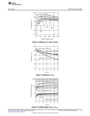
• Measured Efficiency: 95.5% (V
IN
= 6 V, I
OUT
= 200 mA)
• Nominal Switching Frequency: 200 kHz
• Size: 2.25 in. x 0.88 in. x 0.47 in
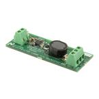
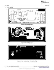
Figure 1. Evaluation Board - Top Side
2 Theory of Operation
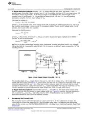
Figure 3 contains a simplified block diagram of the LM25010. When the circuit is in regulation, the buck
switch is on each cycle for a time determined by R1 and V
IN
according to the equation:
(1)
All trademarks are the property of their respective owners.
1
SNVA142A–December 2005–Revised April 2013 AN-1431 LM25010 Evaluation Board
Submit Documentation Feedback
Copyright © 2005–2013, Texas Instruments Incorporated
Verzeichnis
- ・ Blockdiagramm on Seite 4
- ・ Anwendungsbereich on Seite 7