


herunterladen
R1 = R2
- 1
V
OUT
1.238
User's Guide
SNVA019A–October 2007–Revised April 2013
AN-1147 LM2651_EVAL
1.5A High Efficiency Synchronous Switching Regulator
Evaluation Board
1 Introduction
The LM2651 switching regulator provides high efficiency power conversion over a 100:1 load range (1.5A
to 15mA). This feature makes the LM2651 an ideal fit in battery powered applications.
Synchronous rectification and 75 mΩ internal switches provide up to 97% efficiency. At light loads, the
LM2651 enters a low power hysteretic or sleep mode to keep the efficiency high. In many applications, the
efficiency still exceeds 80% at 15 mA load.
A shutdown pin is available to disable the LM2651 and reduce the supply current to 7 µA. The IC contains
patented current sensing circuitry for current mode control. This feature eliminates the external current
sensing required by other current mode DC to DC converters. The IC has a 300kHz fixed frequency
internal oscillator. The high oscillator frequency allows the use of extremely small, low profile components.
The evaluation board can be obtained by ordering part number LM2651_EVAL from your local Texas
Instruments sales office, or TI website at www.ti.com.
2 Evaluation Board Design
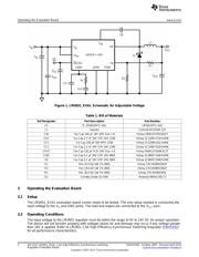
The evaluation board is designed to supply 1.8V, 2.5V, 3.3V or adjustable output voltages at 15 mA up to
1.5A. The evaluation board comes with a design to supply an output voltage of 2.5V with input voltage
range of 4V to 14V and output current range of 15 mA to 1.5A. The design can easily be modified to
provide other output voltage using Equation 1 to change the ratio of the feedback resistors R1 and R2:
(1)
The feedback resistors should not be made arbitrarily large as this would create a high impedance node at
the feedback pin that is more susceptible to noise. A combined value of 50 kΩ for the two resistors is
adequate.
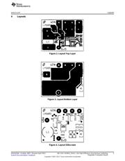
Components were selected based on the design procedure in the LM2651 datasheet. PCB layout is
critical to reduce noise and ensure specified performance for any power supply design. To minimize the
parasitic inductance in the loop of input capacitors and the internal MOSFETs, connect the capacitors to
V
IN
and PGND pins with short and wide traces. This is important because the rapidly switching current,
together with wiring inductance can generate large voltage spikes that may cause noise problems. Locate
the feedback resistors close to the IC and keep the feedback trace as short as possible. Do not run any
feedback traces near the switch node and keep away from the flux field of the inductor. The schematic is
shown in Figure 1. The parts list of the design is shown in Table 1. The pictorial representations of the
layout top, bottom and silkscreen layers are shown at the end of this application note.
When an undervoltage situation occurs, the output voltage can be pulled below ground as the inductor
current is reversed through the synchronous FET. For applications which need to be protected from a
negative voltage, a clamping diode D2 is recommended. When used, D2 should be connected cathode to
V
OUT
and anode to ground. A diode rated for a minimum of 2A is recommended.
All trademarks are the property of their respective owners.
1
SNVA019A–October 2007–Revised April 2013 AN-1147 LM2651_EVAL 1.5A High Efficiency Synchronous Switching
Regulator Evaluation Board
Submit Documentation Feedback
Copyright © 2007–2013, Texas Instruments Incorporated
Verzeichnis
- ・ Blockdiagramm on Seite 2
- ・ Anwendungsbereich on Seite 4