

herunterladen

User's Guide
SNVA345B–November 2008–Revised April 2013
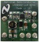
AN-1844 LM2833Z MSOP-PowerPAD Demo Board
1 Introduction
The LM2833Z MSOP-PowerPAD demo board is designed to demonstrate the capabilities of the LM2833Z
3MHz switching regulator in an MSOP PowerPAD-10 package.
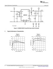
The demo board is configured to provide an output of 1.2V at up to 3A from an input voltage range of 3V
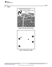
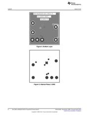
to 5.5V. The board is thermally optimized with the small solution size of 1.2" X 1.1", shown in the demo
board schematic in Figure 1. The output voltage can be configured to a different value by changing the
ratio between R1 and R2 according to the following equation:
R1 = R2 x (VOUT / VFB - 1) (1)
The feedback voltage VFB is regulated at 0.60V typically.
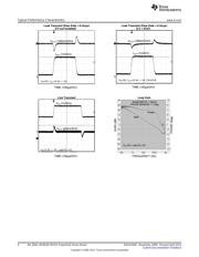
The board has C5 reserved for two purposes given different application scenarios. First, at high VOUT
applications, the control loop bandwidth is not as large as at low VOUT. Adding C5 at high VOUT can
significantly improve the load step response by boosting the loop bandwidth without significantly
compromising phase margin. Secondly, it also helps to minimize output voltage overshoot during sluggish
startup, short circuit release, and recovery from thermal shutdown, since it creates a feed-forward path
between VOUT and VFB, thus speeding up Gm-amplifier recovery. In practice, for a few kΩ of voltage
divider bottom resistor R2, a 47nF ceramic capacitor is usually a good choice for C5. Note for applications
where VOUT is close to VFB, since R1 is small, the effectiveness of adding C5 becomes decreasingly
appreciable. Therefore, other measures need to be taken to achieve the desired performance. For
example, to minimize output overshoot during slow startup at high VOUT, an alternative approach is to
apply a separate signal at the EN terminal after VIN is fully established.
Another component which is not populated on the board is C4, which is reserved for applications where a
large output capacitor is desired.
Table 1 lists the bill of materials of this demo board. The measured performance characteristics and layout
of this board are also included below.
2 Powering up the Board
Powering up the LM2833Z MSOP-PowerPAD demo board is a single-step procedure, simply by applying a
DC voltage of 3V to 5.5V to VIN and GND terminals. By default, VINC is connected to VIN through a low
pass filter to remove any high frequency noise present at the input. EN is connected to VINC through a
100kΩ resistor. A separate logic signal at the EN terminal can be used, if startup and shutdown need to
be controlled. A load can be connected between VOUT and GND terminals before or after the board is
powered up. At VOUT of 1.2V, the internal soft-start circuit can bring up VOUT smoothly regardless of
load or input voltage.
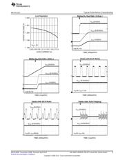
The LM2833Z is designed to skip some pulses at very light loads to maintain output voltage regulation.
Depending on load levels, the circuit may operate in either discontinuous or continuous conduction mode.
All trademarks are the property of their respective owners.
1
SNVA345B–November 2008–Revised April 2013 AN-1844 LM2833Z MSOP-PowerPAD Demo Board
Submit Documentation Feedback
Copyright © 2008–2013, Texas Instruments Incorporated
Verzeichnis