
herunterladen

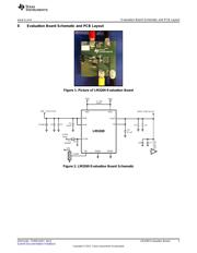
2.2 PH
PVIN
PVIN
EN
SGND PGND
SW1 SW2
LM3269
VOUT
FB
VCON
V
OUT
: 0.6V to 4.2V
4.7 PF
10 PF
V
IN
: 2.7V to 5.5V
GPO1
BB RFIC
DAC
V
OUT
= 3 x VCON
RF
PA
User's Guide
SNVU162–FEBRUARY 2013
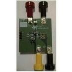
LM3269 Evaluation Board
1 Introduction
The LM3269 evaluation board is a working demonstration of a buck-boost DC-DC converter designed to
generate output voltages above or below a given input voltage. It is particularly suitable for cell-phone
applications powering 3G/4G Power Amplifiers.
For more details and electrical characteristics about the converter operation, please refer to the LM3269
data sheet. If you are considering using the LM3269 in a system design, please review the "PCB Layout
Considerations” section of the data sheet.
2 Operating Conditions
The device will operate under the following conditions:
• V
IN
: 2.7V ≤ V
IN
≤ 5.5V
• Adjustable V
OUT
: 0.6V to 4.2V
• VCON: 0.2V to 1.4V
• V
OUT
equation: V
OUT
= 3 x VCON
• I
OUT
range: 0mA to 750mA
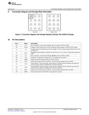
3 Package
The LM3269 is available in a 12-bump (0.4 mm pitch) lead-free DSBGA (2.0mm X 2.5mm X 0.6mm)
package.
4 Typical Application Circuit
1
SNVU162–FEBRUARY 2013 LM3269 Evaluation Board
Submit Documentation Feedback
Copyright © 2013, Texas Instruments Incorporated
Verzeichnis