
herunterladen
15
1
2
16
15
1
2
16
LED1
LED2
OUT
OUT
SW
SW
GND
GND
IN
TX2/INT
TX1/
TORCH
LEDI/NTC
SDA
STROBE
SCL
HWEN
LM3559/
LM3560
IN VL
GND VL
OUT
VI/O
STROBE
VI/O
VUSB
VIN
A2
A1
RTH
LED2
(PWF4)
LED1
(PWF4)
LED3
SDA
GND
SCL
GND
RSDA
(4.7 k:)
RSCL
(4.7 k:)
R_HWEN
(4.7 k:)
CIN
(10 PF)
L
(1 PH)
COUT
(10 PF)
TX1/TORCH
VI/O
VL/VUSB
FLASH
(Button)
R2
(0.1:)
R1
(0.1:)
RBIAS
GND
VBIAS
GND
USBL
USBR
TX2/INT
VI/O
GND
CBYP
LEDI/NTC
GND
GND
SW
HWEN
GND
User's Guide
SNVA439A–September 2011–Revised April 2013
AN-2057 LM3559/LM3560 Evaluation Board
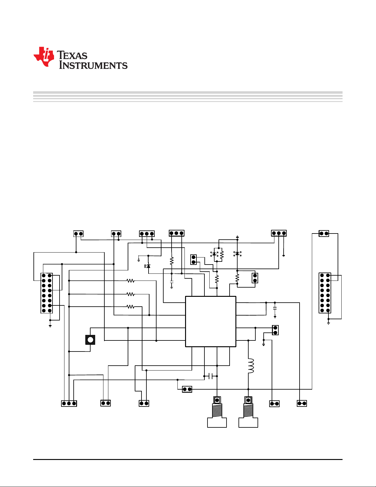
1 Introduction
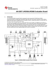
The LM3559/LM3560 Evaluation Board is designed to fully evaluate the LM3559 and LM3560
Synchronous Boost Converter with dual 900mA High Side Flash LED Drivers (LM3559) or dual 1000mA
High Side Flash Drivers (LM3560) and I
2
C-Compatible Interface. Detailed descriptions for either parts can
be found in their device-specific data sheets.
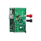
The board comes equipped with two Lumiled Flash LEDs (LXCL-EYW4). An additional LED (LED3) is a
red LED which operates as the message indicator. The on-board flash button demonstrates the hardware
flash feature of the LM3559/LM3560 and, when pushed, the Flash LEDs turn on at their programmed
Flash current. There are two 4.7kΩ pull-up resistors on board for the I
2
C clock and data lines and a 4.7kΩ
pull-up (R_HWEN) that pulls the active high hardware enable pin (HWEN) high. Each Input and/or output
from the LM3559 has its own separate header pin to serve as a test-point.
Figure 1. LM3559/LM3560 Evaluation Board Schematic
All trademarks are the property of their respective owners.
1
SNVA439A–September 2011–Revised April 2013 AN-2057 LM3559/LM3560 Evaluation Board
Submit Documentation Feedback
Copyright © 2011–2013, Texas Instruments Incorporated