
herunterladen
1
®
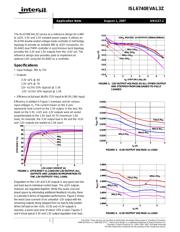
AN1127.2
CAUTION: These devices are sensitive to electrostatic discharge; follow proper IC Handling Procedures.
1-888-INTERSIL or 1-888-468-3774
| Intersil (and design) is a registered trademark of Intersil Americas Inc.
Copyright © Intersil Americas Inc. 2004, 2005, 2007. All Rights Reserved
All other trademarks mentioned are the property of their respective owners.
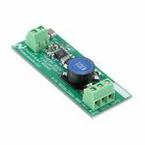
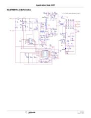
ISL6740EVAL3Z
The ISL6740EVAL3Z serves as a reference design for a 48V
to ±12V, 3.3V and 1.5V isolated power supply. It utilizes an
ISL6740 double-ended voltage mode controller in half bridge
topology to provide an isolated 48V to ±12V conversion. An
ISL6402 dual PWM controller in synchronous buck topology
provides the 3.3V and 1.5V outputs from the +12V rail. The
reference design also provides pads to implement an
optional LDO using the ISL6402 as a controller.
Specifications
• Input Voltage: 36V to 72V
• Outputs:
3.3V ±1% @ 4A
1.5V ±1% @ 7A
12V +3.5%/-10% (typical) @ 1.5A
-12V +3.5%/-10% (typical) @ 1.5A
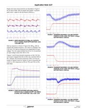
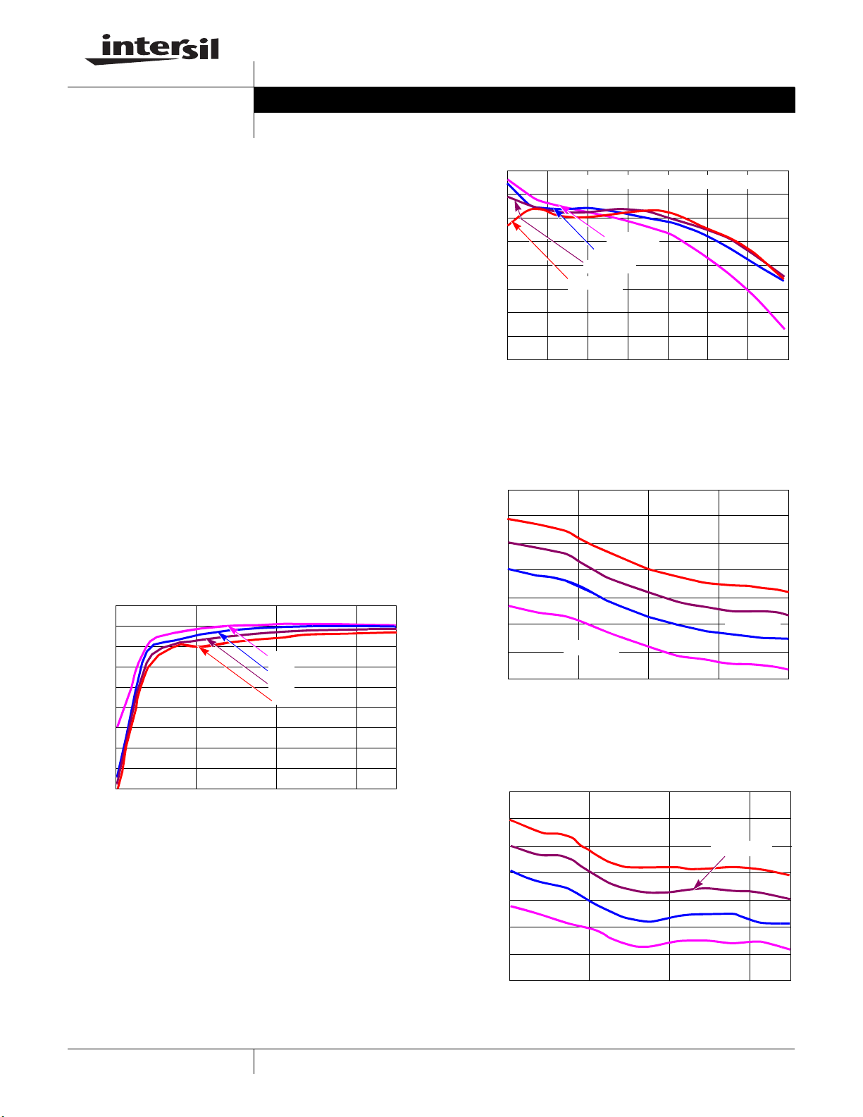
• Efficiency at full load: 86.8% (72V input) to 90.3% (36V input)
Efficiency is plotted in Figure 1 overload, and for various
input voltages V
I
. The current shown on the X axis
represents load current on the 1.5V output. In this test, the
loads on the 3.3V, +12V and -12V outputs were all varied
proportionately to the 1.5V load. At 7A (maximum 1.5A
load), for example, the 3.3V output load is 4A and the +12V
and -12V outputs are loaded at 1.5A each.
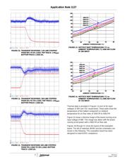
Regulation on the 1.5V and 3.3V outputs is very good over line
and load due to individual control loops. The ±12V outputs,
however, are regulated together. While this saves cost and
board space by eliminating additional feedback circuitry, there
is a penalty in terms of regulation performance. Figure 2 shows
the worst case scenario of an unloaded -12V output with the
remaining outputs being stepped from no load to fully loaded.
When full load on the +12V, +3.3V and +1.5V outputs is
reached, a worst case error of about -10% is seen. Figures 3
and 4 show typical 3.3V and 1.5V output regulation over load.
FIGURE 1. EFFICIENCY vs LOAD ON 1.5V OUTPUT. ALL
OUTPUTS ARE LOADED IN PROPORTION TO
THE 1.5V OUTPUTS’ FULL LOAD.
100
90
80
70
60
50
40
30
20
10
02 4 6
1.5V LOAD CURRENT (A)
EFFICIENCY (%)
36V
I
48V
I
60V
I
72V
I
FIGURE 2. -12V OUTPUT VOLTAGE AS ALL OTHER OUTPU
T
ARE STEPPED FROM UNLOADED TO FULLY
LOADED
-11.8
-12.0
-12.2
-12.4
-12.6
-12.8
-13.0
-13.2
-13.4
0246
V
OUT
(V)
315
7
36V
I
/-12V
O
-12V
O
, REG/DSL 14 OUTPUTS (200kHz/300kHz)
I
O
, STEP ON 1.5V
O
(A)
48V
I
/-12V
O
60V
I
/-12V
O
72V
I
/-12V
O
FIGURE 3. +3.3V OUTPUT VOLTAGE vs LOAD
3.3255
3.3250
3.3245
3.3240
3.3235
3.3230
3.3225
3.3220
012 3
I
O
(A)
V
OUT
(V)
48V
I
/3.3V
O
72V
I
/3.3V
O
4
36V
I
/3.3V
O
60V
I
/3.3V
O
FIGURE 4. +1.5V OUTPUT VOLTAGE vs LOAD
1.4964
1.4962
1.4960
1.4958
1.4956
1.4954
1.4952
1.4950
024 6
I
O
(A)
V
OUT
(V)
36V
I
/1.5V
O
48V
I
/1.5V
O
60V
I
/1.5V
O
72V
I
/1.5V
O
Application Note August 1, 2007
Verzeichnis
- ・ Blockdiagramm on Seite 6 Seite 7
- ・ Technische Daten on Seite 1