

herunterladen
User's Guide
SNVA484A–October 2011–Revised May 2013
AN-2149 LM5113 Evaluation Board
1 Introduction
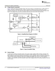
The LM5113 evaluation board is designed to provide the design engineers with a synchronous buck
converter to evaluate the LM5113, a 100V half-bridge enhancement mode Gallium Nitride (GaN) FET
driver. The active clamping voltage mode controller LM5025 is used to generate the PWM signals of the
buck switch and the synchronous switch. The specifications of the evaluation board are as follows:
• Input Operating Voltage: 15V to 60V
• Output Voltage: 10V
• Output Current: 10A @ 48V, 7A @ 60V
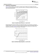
• Measured Efficiency at 48V: 93.9% @ 10A
• Frequency of Operation: 800kHz
• Line UVLO: 13.8V (Rising) /10.8V (Falling)
• Board size: 3.00 x 2.83 inches
The printed circuit board (PCB) consists of 2 layers of 2 ounce copper on FR4 material, with a thickness of
0.050 inches.
This document contains the schematic of the evaluation board, Bill of Materials (BOM) and a quick setup
procedure. The evaluation board can be reconfigured for different switching frequency, dead time, and the
output voltage from the specifications above. An example of 48V to 3.3V conversion is given in
Appendix A. For more complete information, see the LM5113 5A, 100V Half-Bridge Gate Driver for
Enhancement Mode GaN FETs Data Sheet (SNVS725)
2 IC Features
• Independent high-side and low-side TTL logic inputs
• 1.2A/5A peak source/sink current
• High-side floating bias voltage rail operates up to 100VDC
• Internal bootstrap supply voltage clamping
• Split outputs for adjustable turn-on/turn-off strength
• 0.6Ω/2.1Ω pull-down/pull-up resistance
• Fast propagation times (28 ns typical)
• Excellent propagation delay matching (1.5 ns typical)
• Supply rail under-voltage lockout
• Low power consumption
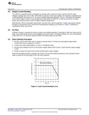
3 Powering and Loading Considerations
Certain precautions need to be followed when applying power to the LM5113 evaluation board. A
misconnection can damage the assembly.
All trademarks are the property of their respective owners.
1
SNVA484A–October 2011–Revised May 2013 AN-2149 LM5113 Evaluation Board
Submit Documentation Feedback
Copyright © 2011–2013, Texas Instruments Incorporated
Verzeichnis